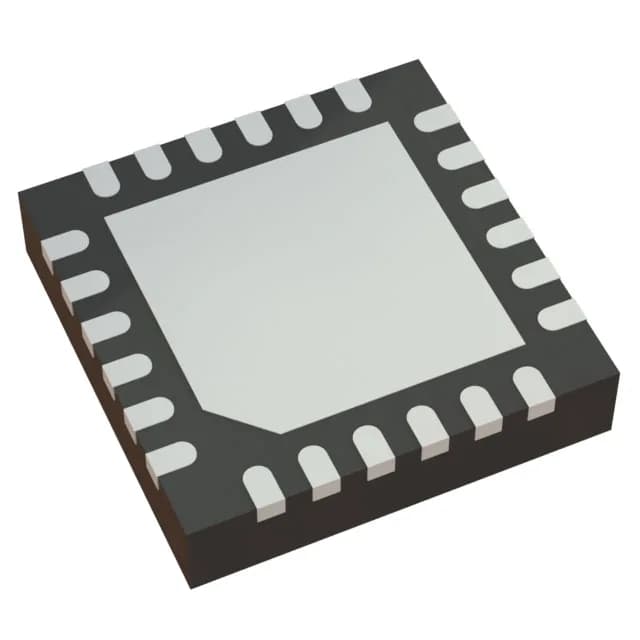
Renesas Electronics RC32504A000GNK#BB0 — Discrete Semiconductors

Renesas RC32504A000GNK#BB0 FemtoClock Frequency Translator

MPNRC32504A000GNK#BB0
End of Life

Renesas FemtoClock® RC32504A000GNK#BB0, PLL-based Frequency Translator, 2:5 ratio, differential I/O, 180 MHz / 1 GHz max, 1.71V–1.89V / 3.465V supply, -40 to 85°C, 24-VFQFPN (4x4).

$15.0Ref. price · indicative, final on quote
Packaging24-WFQFN Exposed Pad
StockContact for availability
MOQ1 pcs
  • 100% new & originalTraceable channels only — no refurbs, no pulls, no remarked parts.
  • Date & lot codes on quoteStated per line before you commit; label photos on request.
  • MSL-compliant ESD packingMoisture-sealed bags with indicator cards; reels photo-verified.
  • PayPal buyer protectionPay by T/T, PayPal or Payoneer — card payments covered end to end.

Specifications

RC32504A000GNK#BB0 Technical Specifications
ParameterValue
TypeFrequency Translator
SeriesFemtoClock®
Mounting typeSurface Mount
Voltage1.71V ~ 1.89V, 3.465V
Frequency180MHz, 1GHz
Operating temperature-40°C ~ 85°C (TA)
PLLYes
InputHCSL, LVCMOS, LVDS, Crystal
OutputCML, HCSL, LVCMOS, LVDS, LVPECL
PackageTray
Case24-WFQFN Exposed Pad
Divider (Multiplier)Yes/No
Number of circuits1
Ratio - Input:Output2:5
Differential - Input:OutputYes/Yes

Product details

PLL frequency translator for precision clock trees

The Renesas RC32504A000GNK#BB0 is a FemtoClock® PLL-based frequency translator that accepts HCSL, LVCMOS, LVDS, or crystal inputs and delivers up to five outputs in CML, HCSL, LVCMOS, LVDS, or LVPECL formats. It operates from a 1.71 V to 1.89 V core supply plus a 3.465 V I/O rail, and is rated over the -40°C to 85°C industrial temperature range. This part is designed for clock conditioning in networking, base-station, and FPGA-based systems where jitter cleaning and format conversion are required.

Dual frequency maximums — which one applies

The frequency maximum is listed at both 180 MHz and 1 GHz. The 1 GHz figure applies to the differential output paths (CML, LVPECL, LVDS), while the 180 MHz limit governs the LVCMOS single-ended outputs.

Supply sequencing matters

Two separate supply domains — a 1.71 V to 1.89 V core and a 3.465 V I/O rail — mean the board designer must sequence or at least ensure both are clean before the PLL locks.

Lifecycle and sourcing

It is ROHS3 compliant. No official replacement or second-source alternate is recorded — this is the current FemtoClock device for this configuration.

Frequently asked questions

What input and output signal types does the RC32504A000GNK#BB0 support?

The RC32504A000GNK#BB0 accepts HCSL, LVCMOS, LVDS, or crystal inputs and outputs CML, HCSL, LVCMOS, LVDS, or LVPECL. All inputs and outputs are differential-capable.

What is the frequency range of the RC32504A000GNK#BB0?

The RC32504A000GNK#BB0 has a maximum frequency of 1 GHz on differential outputs and 180 MHz on LVCMOS outputs.