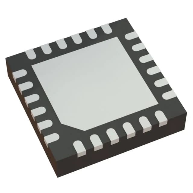
Renesas Electronics RC22504A000GNK#BB0 — Discrete Semiconductors

RC22504A000GNK#BB0 FemtoClock Frequency Synthesizer

MPNRC22504A000GNK#BB0
End of Life

Renesas FemtoClock® RC22504A000GNK#BB0 frequency synthesizer, PLL Yes, input Clock/Crystal, output CML/HCSL/LVCMOS/LVDS/LVPECL, frequency max 180 MHz / 1 GHz, 2:5 ratio, 1.71V–1.89V / 3.465V supply, -40°C to 85°C, 24-VFQFPN (4x4) tray.

$14.42Ref. price · indicative, final on quote
Packaging24-WFQFN Exposed Pad
StockContact for availability
MOQ1 pcs
  • 100% new & originalTraceable channels only — no refurbs, no pulls, no remarked parts.
  • Date & lot codes on quoteStated per line before you commit; label photos on request.
  • MSL-compliant ESD packingMoisture-sealed bags with indicator cards; reels photo-verified.
  • PayPal buyer protectionPay by T/T, PayPal or Payoneer — card payments covered end to end.

Specifications

RC22504A000GNK#BB0 Technical Specifications
ParameterValue
TypeFrequency Synthesizer
SeriesFemtoClock®
Mounting typeSurface Mount
Voltage1.71V ~ 1.89V, 3.465V
Frequency180MHz, 1GHz
Operating temperature-40°C ~ 85°C (TA)
PLLYes
InputClock, Crystal
OutputCML, HCSL, LVCMOS, LVDS, LVPECL
PackageTray
Case24-WFQFN Exposed Pad
Divider (Multiplier)Yes/No
Number of circuits1
Ratio - Input:Output2:5
Differential - Input:OutputYes/Yes

Product details

FemtoClock frequency synthesizer — one part, five output families

The Renesas RC22504A000GNK#BB0 is a FemtoClock® PLL-based frequency synthesizer that takes a single clock or crystal input and generates up to five synchronized output clocks. The PLL locks to the reference and synthesizes frequencies up to 180 MHz on the LVCMOS paths and up to 1 GHz on the differential outputs (CML, HCSL, LVDS, LVPECL). The 2:5 input-to-output ratio gives you one redundant reference input for failover or a clean crystal port, and five outputs you can assign across the differential and single-ended families. The industrial temperature range (-40°C to 85°C) suits base-station, industrial Ethernet switch, and test-equipment clock trees.

1 GHz differential outputs — which SERDES lanes it feeds

The PLL's jitter performance (not quantified in this listing) is the deciding factor for high-speed SERDES — verify the phase-noise plot in the datasheet against your link budget.

24-VFQFPN footprint — layout and thermal notes

The 24-VFQFPN (4x4 mm) exposed-pad package requires a thermal via array under the center pad for adequate heat transfer to the ground plane. The pad is electrically connected to the die substrate — typically ground.

Frequently asked questions

What is the maximum output frequency of RC22504A000GNK#BB0?

The maximum output frequency is 1 GHz on the differential outputs (CML, HCSL, LVDS, LVPECL) and 180 MHz on the LVCMOS outputs.

Does RC22504A000GNK#BB0 work with 1.8V supply voltage?

Yes, the core supply range is 1.71 V to 1.89 V, which covers a nominal 1.8 V rail. The I/O supply is 3.465 V nominal.

Is RC22504A000GNK#BB0 compatible with 3.3V CMOS logic?

Yes, the I/O supply rail is 3.465 V, which is within the 3.3 V logic family. The LVCMOS output type is directly compatible with 3.3 V CMOS inputs.