Renesas Electronics R5F566TFCGFB#30 — DC-DC Power Modules

Renesas R5F566TFCGFB#30 RXv3 32-bit MCU, 160 MHz

MPNR5F566TFCGFB#30
End of Life

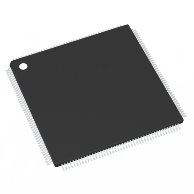
Renesas RX R5F566TFCGFB#30, 32-bit RXv3 MCU, 160 MHz, 512 KB Flash, 128 KB RAM, 32 KB EEPROM, 110 I/O, 144-LQFP, -40°C to 105°C, 2.7 V to 5.5 V.

$8.6Ref. price · indicative, final on quote
Packaging144-LQFP
StockContact for availability
MOQ1 pcs
  • 100% new & originalTraceable channels only — no refurbs, no pulls, no remarked parts.
  • Date & lot codes on quoteStated per line before you commit; label photos on request.
  • MSL-compliant ESD packingMoisture-sealed bags with indicator cards; reels photo-verified.
  • PayPal buyer protectionPay by T/T, PayPal or Payoneer — card payments covered end to end.

Specifications

R5F566TFCGFB#30 Technical Specifications
ParameterValue
SeriesRX
Mounting typeSurface Mount
Oscillator typeInternal
Program memory typeFLASH
Voltage - supply (Vcc (Vdd))2.7V ~ 5.5V
Operating temperature-40°C ~ 105°C (TA)
Speed160MHz
PackageTray
RAM size128K x 8
Core size32-Bit
EEPROM size32K x 8
PeripheralsDMA, LVD, POR, PWM, WDT
ConnectivityCANbus, EBI/EMI, I²C, LINbus, MMC/SD, SCI, SPI, SSI, UART/USART, USB
Number of i (O)110
Core processorRXv3
Case144-LQFP
Data convertersA/D 30x12b; D/A 2x12b
Program memory size512KB (512K x 8)

Product details

RXv3 core at 160 MHz — what that means for the control loop

The Renesas R5F566TFCGFB#30 is a 32-bit RXv3 microcontroller running at 160 MHz, built for deterministic real-time control in industrial and automotive-adjacent applications. The 512 KB on-chip Flash and 128 KB RAM hold a substantial firmware image and data buffers without external memory, while the 32 KB dedicated EEPROM block stores calibration constants and configuration parameters that survive power cycles. With 110 I/O lines in a 144-pin LQFP, this part suits parallel display interfaces, large sensor arrays, or multi-axis motion control where pin count is the binding constraint.

Connectivity and analog density

The peripheral set includes CANbus, USB, SCI/UART, SPI, I²C, and an EBI/EMI bus. The 30-channel 12-bit ADC and two 12-bit DACs handle analog I/O. Supply range is 2.7 V to 5.5 V.

Temperature grade and deployment envelope

Rated for -40°C to 105°C ambient, this MCU is specified for factory-floor enclosures, outdoor telecom cabinets, and under-hood electronics where the junction temperature climbs. The internal oscillator eliminates the external crystal for cost-sensitive builds, though the EBI/EMI bus and USB PHY still benefit from a precision clock source when timing margin is tight.

Lifecycle and sourcing posture

That means it remains a valid selection for new production builds and ongoing BOM lines. No stock or price figures are published here because the channel position changes daily — submit an RFQ for the real-time picture.

Frequently asked questions

Does R5F566TFCGFB#30 have a CAN bus interface?

Yes, the connectivity block includes CANbus, along with USB, I²C, SPI, SCI, LINbus, and an EBI/EMI bus for external memory or FPGA.

What is the maximum clock speed of R5F566TFCGFB#30?

The RXv3 core runs at 160 MHz, which is the maximum rated speed for this device.

Does R5F566TFCGFB#30 have a built-in ADC?

Yes, the part integrates a 30-channel 12-bit ADC and a 2-channel 12-bit DAC for analog signal acquisition and output.

What is the equivalent of R5F566TFCGFB#30?

The closest functional sibling is the R5F566TAAGFP#30, which shares the same RXv3 core at 160 MHz and the same peripheral set (CAN, USB, serial, DMA, PWM) but in a 100-pin package with 72 I/O and 22 ADC channels. The R5F566TFCGFB#30 offers more I/O (110 vs 72) and more ADC channels (30 vs 22) in the larger 144-pin LQFP. Neither is a drop-in replacement — the pin count and footprint differ — but the code base and peripheral register map are compatible across the RX66T family.