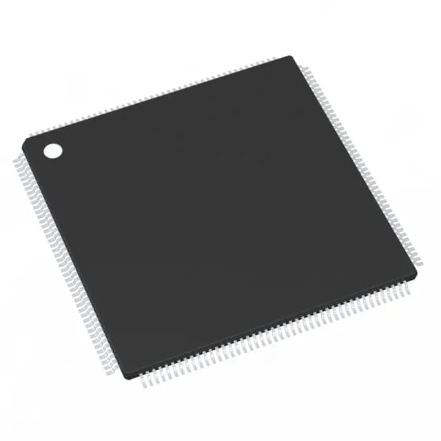
Renesas Electronics R5F56609BGFB#30 — Analog & Data Acquisition

R5F56609BGFB#30 RXv3 MCU, 120 MHz, 1 MB Flash, 144-LFQFP

MPNR5F56609BGFB#30
End of Life

Renesas RX600 series, R5F56609BGFB#30, 32-Bit RXv3 MCU, 120 MHz, 1MB (1M x 8) FLASH, 128K x 8 RAM, 32K x 8 EEPROM, 133 I/O, CANbus, I²C, SPI, SCI, LIN, EBI/EMI, 24x12b ADC, 2x12b DAC, -40°C to 105°C, 144-LFQFP, Tray.

$8.4Ref. price · indicative, final on quote
Packaging144-LQFP
StockContact for availability
MOQ1 pcs
  • 100% new & originalTraceable channels only — no refurbs, no pulls, no remarked parts.
  • Date & lot codes on quoteStated per line before you commit; label photos on request.
  • MSL-compliant ESD packingMoisture-sealed bags with indicator cards; reels photo-verified.
  • PayPal buyer protectionPay by T/T, PayPal or Payoneer — card payments covered end to end.

Specifications

R5F56609BGFB#30 Technical Specifications
ParameterValue
SeriesRX600
Mounting typeSurface Mount
Oscillator typeExternal, Internal
Program memory typeFLASH
Voltage - supply (Vcc (Vdd))2.7V ~ 5.5V
Operating temperature-40°C ~ 105°C (TA)
Speed120MHz
PackageTray
RAM size128K x 8
Core size32-Bit
EEPROM size32K x 8
PeripheralsDMA, LVD, POR, PWM, WDT
ConnectivityCANbus, EBI/EMI, I²C, LINbus, SCI, SPI
Number of i (O)133
Core processorRXv3
Case144-LQFP
Data convertersA/D 24x12b; D/A 2x12b
Program memory size1MB (1M x 8)

Product details

RXv3 core at 120 MHz — what the speed rating buys you

The Renesas R5F56609BGFB#30 is a 32-bit microcontroller built around the RXv3 CPU core, clocked at 120 MHz. That clock rate, combined with a single-cycle multiply and hardware divide, pushes real-time loop closure in motor-drive and power-conversion applications without an external DSP or FPGA. The 1 MB on-chip Flash and 128 KB RAM (organized as 128K x 8) keep the BOM lean for control firmware that would otherwise spill into external memory.

Memory map and on-chip storage

Program memory is 1 MB of Flash (1M x 8), enough for a full Modbus TCP stack, a CANopen node, and a PID loop with logging. The 32 KB EEPROM (32K x 8) handles calibration constants and fault logs without wear-leveling concerns — it is true EEPROM, not emulated Flash. The 128 KB SRAM (128K x 8) supports multiple frame buffers or a small RTOS heap.

Analog and peripheral density

Twenty-four 12-bit ADC channels and two 12-bit DAC channels cover current-sense, voltage-monitor, and setpoint-output needs on a single chip. The peripheral set includes DMA, LVD, POR, PWM, and WDT — enough to run a safety watchdog and a PWM-driven H-bridge without external glue logic.

Temperature grade and operating environment

Rated for -40°C to 105°C ambient. Supply range is 2.7 V to 5.5 V.

Lifecycle and compliance

ROHS3 compliant. No last-time-buy risk for new designs.

Frequently asked questions

What is the maximum operating frequency of R5F56609BGFB#30?

The core runs at 120 MHz. That clock rate drives the RXv3 pipeline for single-cycle multiply and hardware divide operations.

Is R5F56609BGFB#30 RoHS compliant?

Yes, it is ROHS3 Compliant.

What are the key differences between R5F56609BGFB#30 and STM32F407IGT6?

Both are 32-bit MCUs, but the R5F56609BGFB#30 uses the RXv3 core at 120 MHz with 1 MB Flash and 128 KB RAM, while the STM32F407IGT6 uses an ARM Cortex-M4F at 168 MHz with 1 MB Flash and 192 KB RAM plus a floating-point unit. The RX600 part includes 32 KB true EEPROM and a 2.7 V to 5.5 V supply range — the STM32 runs on 1.8 V to 3.6 V. Package and peripheral sets differ; a board spin is required for a direct swap.