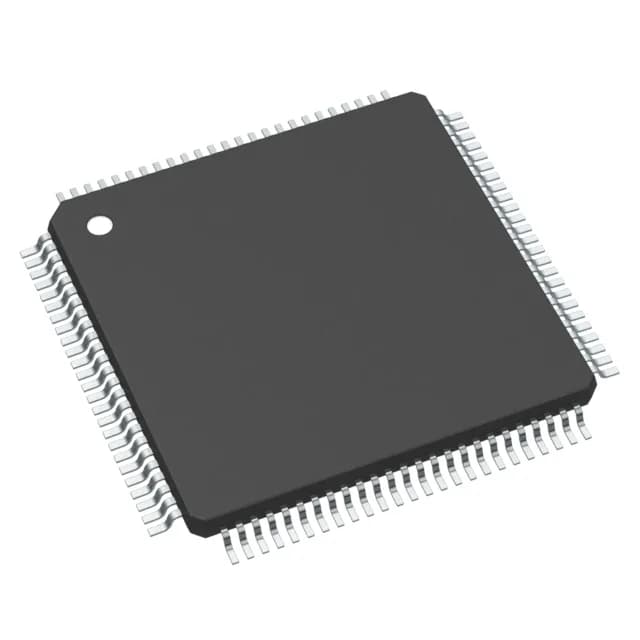
Renesas Electronics R5F565N7AGFP#30 — Analog & Data Acquisition

Renesas R5F565N7AGFP#30 RX65N MCU, 120 MHz RXv2

MPNR5F565N7AGFP#30
End of Life

Renesas RX65N series 32-bit MCU, R5F565N7AGFP#30, RXv2 core at 120 MHz, 768 KB Flash, 256 KB RAM, Ethernet + CAN + USB, 78 I/O, 100-LQFP, -40 to 105°C, ROHS3 compliant.

$7.33Ref. price · indicative, final on quote
Packaging100-LQFP
StockContact for availability
MOQ1 pcs
  • 100% new & originalTraceable channels only — no refurbs, no pulls, no remarked parts.
  • Date & lot codes on quoteStated per line before you commit; label photos on request.
  • MSL-compliant ESD packingMoisture-sealed bags with indicator cards; reels photo-verified.
  • PayPal buyer protectionPay by T/T, PayPal or Payoneer — card payments covered end to end.

Specifications

R5F565N7AGFP#30 Technical Specifications
ParameterValue
SeriesRX65N
Mounting typeSurface Mount
Oscillator typeExternal
Program memory typeFLASH
Voltage - supply (Vcc (Vdd))2.7V ~ 3.6V
Operating temperature-40°C ~ 105°C (TA)
Speed120MHz
PackageTray
RAM size256K x 8
Core size32-Bit
PeripheralsDMA, LVD, POR, PWM, WDT
ConnectivityCANbus, EBI/EMI, Ethernet, I²C, LINbus, MMC/SD, QSPI, SCI, SPI, UART/USART, USB
Number of i (O)78
Core processorRXv2
Case100-LQFP
Data convertersA/D 22x12b; D/A 1x12b
Program memory size768KB (768K x 8)

Product details

RX65N at 120 MHz — what the peripheral set buys you

The Renesas R5F565N7AGFP#30 is a 32-bit RX65N microcontroller built around the RXv2 core running at 120 MHz, with 768 KB of Flash and 256 KB of RAM. The peripheral list — Ethernet MAC, CAN 2.0B, USB 2.0 full-speed, QSPI, and multiple SCI/SPI/I²C channels — targets designs that need a single-chip gateway between an industrial fieldbus and an IP network. The 22-channel 12-bit ADC lets one MCU sample current feedback, voltage rails, and temperature sensors in a motor-drive or servo application without an external analog mux.

768 KB of program Flash gives room for a full TCP/IP stack, a CANopen or EtherCAT slave library, and a modest application layer without external memory. The 256 KB RAM is split between the CPU local SRAM and the Ethernet buffer area; a firmware engineer should budget the DMA descriptors and packet buffers against the RAM map early in the bring-up, because the Ethernet controller can consume several tens of kilobytes in descriptor rings alone.

Package and footprint — 100-LQFP

The 100-LQFP (14x14 mm body) with 0.5 mm pitch is a standard two-layer-routable footprint. 78 general-purpose I/O are available; the remaining pins are taken by power, ground, and the oscillator. The supplier device package is a 100-LFQFP — same footprint, same land pattern. The tray shipping medium means the parts arrive in antistatic trays, not tape-and-reel, so plan for pick-and-place feeder changeover if your line is set up for embossed tape.

Frequently asked questions

What is the closest functional equivalent to R5F565N7AGFP#30?

The R5F565N9BGFB#30 is a higher-I/O sibling in the same RX65N family: it offers 111 I/O, 29 ADC channels, and two DAC channels versus the 78 I/O and 22 ADC channels on this part. Both run the RXv2 core at 120 MHz and share the same Ethernet + CAN + USB peripheral set. The package differs — the R5F565N9BGFB#30 comes in a 144-LQFP — so a board respin is needed to swap between them.

Is R5F565N7AGFP#30 RoHS compliant?

Yes. The part is listed as ROHS3 Compliant.