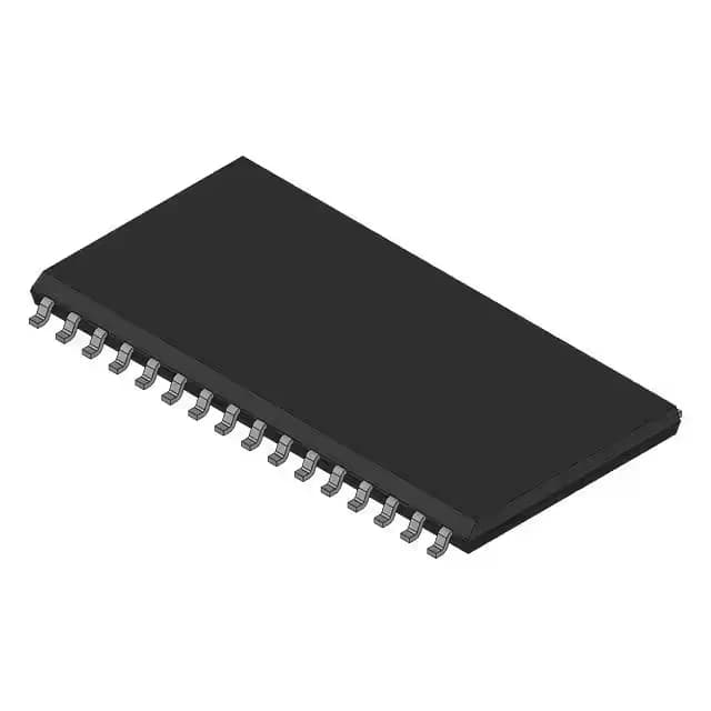
Renesas Electronics R1LP0408DSB-5SI#B0 — Analog & Data Acquisition

R1LP0408DSB-5SI#B0 SRAM 4Mbit Parallel 55ns 32-TSOP II

MPNR1LP0408DSB-5SI#B0
End of Life

R1LP0408DSB-5SI#B0, 4Mbit (512K x 8) Parallel SRAM, 55 ns access time, 4.5V–5.5V supply, -40°C to 85°C, 32-TSOP II surface-mount package.

$15.31Ref. price · indicative, final on quote
Packaging32-SOIC (0.400", 10.16mm Width)
StockContact for availability
MOQ1 pcs
  • 100% new & originalTraceable channels only — no refurbs, no pulls, no remarked parts.
  • Date & lot codes on quoteStated per line before you commit; label photos on request.
  • MSL-compliant ESD packingMoisture-sealed bags with indicator cards; reels photo-verified.
  • PayPal buyer protectionPay by T/T, PayPal or Payoneer — card payments covered end to end.

Specifications

R1LP0408DSB-5SI#B0 Technical Specifications
ParameterValue
Memory typeVolatile
Mounting typeSurface Mount
Voltage4.5V ~ 5.5V
Memory interfaceParallel
Operating temperature-40°C ~ 85°C (TA)
PackageBulk
TechnologySRAM
Access time55 ns
Memory size4Mbit
Memory formatSRAM
Case32-SOIC (0.400\", 10.16mm Width)
Memory organization512K x 8
Write cycle time - word, page55ns

Product details

4 Mbit parallel SRAM for 5 V legacy and industrial designs

The R1LP0408DSB-5SI#B0: 4 Mbit static RAM organized as 512 K x 8 bits, accessed through a parallel interface with a 55 ns access time. It operates from a single 4.5 V to 5.5 V supply rail and is specified over the industrial temperature range of -40°C to 85°C. The memory is volatile. It comes in a 32-TSOP II surface-mount package.

Package and footprint note

The package is a 32-TSOP II with a 0.400-inch (10.16 mm) body width. Verify your PCB land pattern before committing the layout. The part is surface-mount only.

Lifecycle and sourcing posture

No LTB risk to plan around. No official second-source alternate is listed in the record.

Frequently asked questions

Does R1LP0408DSB-5SI#B0 require a 5V supply or can it run at 3.3V?

This SRAM requires a 4.5 V to 5.5 V supply rail. It will not operate from a 3.3 V supply. If your design uses a 3.3 V memory bus, this part is not compatible.

What is the access time of R1LP0408DSB-5SI#B0?

The access time is 55 ns for both read and write cycles. This is the time from address valid to data valid on the parallel bus.

What is a suitable replacement for R1LP0408DSB-5SI#B0?

No official replacement or second-source alternate is listed in the record for this exact order code. Functionally similar 4 Mbit parallel SRAMs in 32-TSOP II from other manufacturers exist, but pin compatibility and timing must be verified against your specific memory controller before substituting.