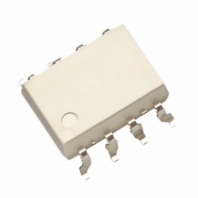
Isolated gate driver for IGBTs and MOSFETs in power-conversion stages
The PS9531L3-V-E3-AX: The PS9531L3-V--AX is a single-channel optical coupling gate driver for IGBTs and power MOSFETs. It transmits a switching signal across a reinforced isolation barrier. The 5000Vrms isolation rating covers safety spacing in motor drives, UPS, and solar inverters. The part carries CSA, SEMKO, UL, and VDE approvals.
2.5 A peak output and 2 A source-sink — sizing the gate drive for medium-power switches
With a peak output rating of 2.5 A and a continuous source/sink capability of 2 A, this driver sits in the mid-range tier of isolated gate drivers. The 40 ns typical rise and fall times keep switching losses manageable. The 175 ns maximum propagation delay and 75 ns maximum pulse width distortion matter when the dead-time budget is tight.
A minimum common-mode transient immunity of 50 kV/µs tells you the output side can tolerate fast voltage slewing at the switching node without corrupting the gate signal. In a hard-switched IGBT inverter, the collector voltage can rise at tens of kV/µs during turn-off. The 50 kV/µs rating here is adequate for most IGBT-based designs.
Supply range and forward diode — biasing the input and output sides
The output-side supply range is 15 V to 30 V, which covers the standard gate-drive voltages for IGBTs and MOSFETs.
Package and temperature grade — board-level fit
The PS9531L3-V--AX comes in an 8-SMD gull-wing package with a 8-SMD supplier device package designation. It is a surface-mount part intended for reflow assembly. The ROHS3 compliance is current. Cut Tape quantities are also available for prototyping or low-volume builds.
The PS9531L3-V--AX carries an active lifecycle status.