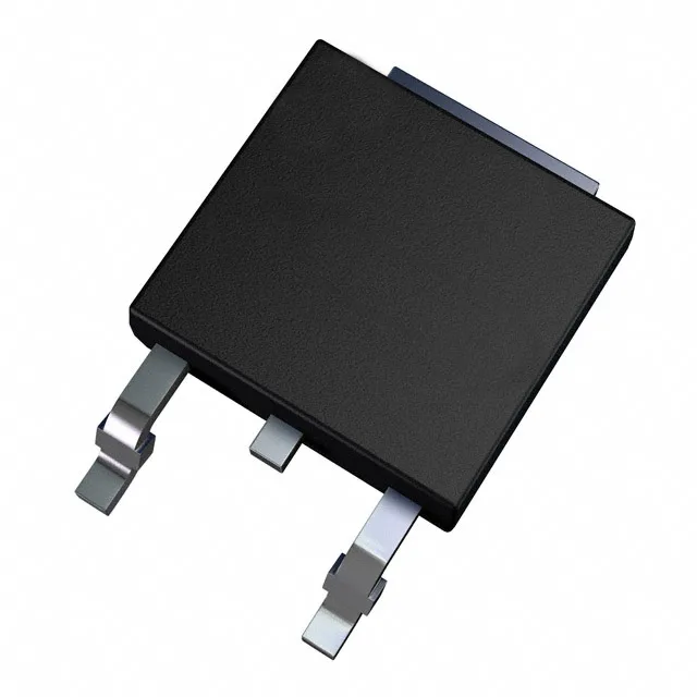
Renesas Electronics NP50P06SDG-E1-AY

NP50P06SDG-E1-AY P-Channel MOSFET, 60V 50A, 16.5mOhm

MPNNP50P06SDG-E1-AY
End of Life

Renesas NP50P06SDG--AY, P-Channel MOSFET, 60 Vdss, 50 A Id, 16.5 mOhm Rds(on) @ 10 V, TO-252-3 (DPak) surface mount, 175 °C junction temperature.

$2.23Ref. price · indicative, final on quote
PackagingTO-252-3, DPak (2 Leads + Tab), SC-63
StockContact for availability
MOQ1 pcs
  • 100% new & originalTraceable channels only — no refurbs, no pulls, no remarked parts.
  • Date & lot codes on quoteStated per line before you commit; label photos on request.
  • MSL-compliant ESD packingMoisture-sealed bags with indicator cards; reels photo-verified.
  • PayPal buyer protectionPay by T/T, PayPal or Payoneer — card payments covered end to end.

Specifications

NP50P06SDG-E1-AY Technical Specifications
ParameterValue
FET typeP-Channel
Mounting typeSurface Mount
Drain to source voltage60 V
Current - continuous drain (Id) @ 25°C50A (Tc)
Power dissipation1.2W (Ta), 84W (Tc)
Operating temperature175°C (TJ)
PackageTape & Reel (TR); Cut Tape (CT)
TechnologyMOSFET (Metal Oxide)
CaseTO-252-3, DPak (2 Leads + Tab), SC-63
Vgs(th) (Max) @ id2.5V @ 250µA
Rds on (Max) @ id, vgs16.5mOhm @ 25A, 10V
Gate charge (Qg) (Max) @ vgs100 nC @ 10 V
Input capacitance (Ciss) (Max) @ vds5000 pF @ 10 V

Product details

Active P-Channel power switch — 60 V, 50 A, 16.5 mOhm

The NP50P06SDG-E1-AY: The Renesas NP50P06SDG--AY is a P-Channel power MOSFET rated at 60 V drain-to-source with a continuous drain current of 50 A at 25 °C case temperature. Gate charge is specified at 100 nC max at 10 V, which tells the drive circuit designer what peak current the gate driver needs to hit the target switching frequency. The 5000 pF input capacitance at 10 V drain bias confirms the gate drive impedance should be kept low to avoid slew-rate limiting.

TO-252-3 package — the tab is the thermal path

This comes in a TO-252-3 (DPak) surface-mount package with the exposed tab as the drain connection and the primary heat path. The power dissipation rating splits sharply: 1.2 W in still air at 25 °C ambient, but 84 W when the tab is soldered to a sufficient copper area on the PCB and the case temperature is held at 25 °C. That 84 W figure assumes a thermal design that pulls heat from the tab into the board — without that copper plane the part thermally throttles well before its current rating. Operating junction temperature is rated to 175 °C, which is the standard ceiling for automotive-grade silicon. The 2.5 V threshold voltage at 250 µA drain current means a 5 V logic gate drive will turn it on hard, though the 16.5 mOhm spec is guaranteed at 10 V.

No official second-source cross-reference is listed in the manufacturer documentation, so dual-sourcing would require qualification of an alternative P-channel part with matching Rds(on) and gate charge.

Frequently asked questions

What compliance documentation does NP50P06SDG--AY carry?

The part is ROHS3 compliant, meaning it meets the RoHS directive including the four phthalates (DEHP, BBP, DBP, DIBP). No REACH or UL certification is listed in the available documentation.

Will NP50P06SDG--AY drop into a board originally designed for NP179N055TUK--AY?

No — the NP179N055TUK--AY is an N-Channel MOSFET, while the NP50P06SDG--AY is P-Channel. The polarity difference means the gate drive and load connections are reversed; they are not pin-compatible or functionally interchangeable without a board redesign.