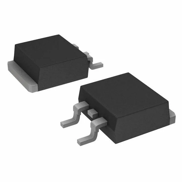
P-channel 40 V switch — conduction loss and thermal budget
The NP50P04KDG-E1-AY: The NP50P04KDG--AY P-Channel MOSFET has a 10 mOhm maximum on-resistance at 25 A, 10 V gate drive.
Rds(on) and gate drive — what 10 mOhm at 10 V means for your BOM
With Rds(on) specified at 10 V gate drive, this FET requires a gate voltage above 10 V to reach its minimum on-resistance. The drive voltage range listed as 4.5 V to 10 V means the device will turn on at 4.5 V but with higher Rds(on); for the rated 10 mOhm, plan on a 10 V gate rail. At 50 A continuous, the conduction loss at 10 mOhm is 25 W — the TO-263 package with exposed tab can handle 90 W at the case, but the 1.8 W at ambient rating means a heatsink or PCB copper plane is mandatory for any load above a few amps.
Switching and gate charge — sizing the driver
Package and thermal — TO-263 land pattern notes
The TO-263-3 (D²Pak) package has two leads plus the exposed tab. For 50 A continuous, a minimum 2 oz copper pour of several square inches on the top layer, with thermal vias to an internal or bottom-layer plane, keeps the junction temperature below 175 °C.
It is ROHS3 compliant.