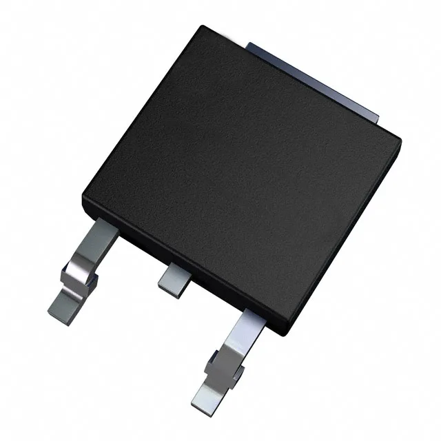
Renesas Electronics NP20P04SLG-E1-AY

NP20P04SLG-E1-AY P-Channel MOSFET, 40 V, 20 A, TO-252

MPNNP20P04SLG-E1-AY
End of Life

Renesas NP20P04SLG--AY, P-Channel MOSFET, 40 V Vdss, 20 A continuous drain, 25 mOhm Rds(on) at 10 A, 10 V, TO-252-3 (DPak) package, Surface Mount.

$1.5Ref. price · indicative, final on quote
PackagingTO-252-3, DPak (2 Leads + Tab), SC-63
StockContact for availability
MOQ1 pcs
  • 100% new & originalTraceable channels only — no refurbs, no pulls, no remarked parts.
  • Date & lot codes on quoteStated per line before you commit; label photos on request.
  • MSL-compliant ESD packingMoisture-sealed bags with indicator cards; reels photo-verified.
  • PayPal buyer protectionPay by T/T, PayPal or Payoneer — card payments covered end to end.

Specifications

NP20P04SLG-E1-AY Technical Specifications
ParameterValue
FET typeP-Channel
Mounting typeSurface Mount
Drain to source voltage40 V
Drive voltage (Max rds on, min rds on)4.5V, 10V
Current - continuous drain (Id) @ 25°C20A (Tc)
Power dissipation1.2W (Ta), 38W (Tc)
Operating temperature175°C (TJ)
PackageTape & Reel (TR); Cut Tape (CT)
Vgs±20V
TechnologyMOSFET (Metal Oxide)
CaseTO-252-3, DPak (2 Leads + Tab), SC-63
Vgs(th) (Max) @ id2.5V @ 250µA
Rds on (Max) @ id, vgs25mOhm @ 10A, 10V
Gate charge (Qg) (Max) @ vgs34 nC @ 10 V
Input capacitance (Ciss) (Max) @ vds1650 pF @ 10 V

Product details

The NP20P04SLG-E1-AY: The NP20P04SLG--AY is a 40 V, 20 A P-Channel power MOSFET from Renesas in the standard TO-252-3 (DPak) surface-mount package. The 40 V drain-to-source breakdown voltage gives 20 % headroom on a 12 V rail and clears a 24 V nominal bus with margin.

On-resistance and gate drive — the efficiency trade-off

Maximum Rds(on) is 25 mOhm at 10 A drain current with 10 V applied to the gate. That is the conduction loss floor for a hard-switched load: at 10 A the dissipation is 2.5 W, which the TO-252 can handle with a reasonable copper area on the drain tab. The gate threshold voltage is 2.5 V max at 250 µA, so the part turns on fully with 4.5 V logic-level drive, but the lowest Rds(on) is achieved at 10 V gate drive. Total gate charge is 34 nC at 10 V. The 1650 pF input capacitance at 10 V Vds influences switching loss at higher frequencies.

Thermal limits and package reality

Maximum junction temperature is 175 °C — typical for automotive-grade silicon, though this part is not listed with AEC-Q101 qualification. The power dissipation is rated 1.2 W at 25 °C ambient (no heatsink) and 38 W at 25 °C case temperature with the tab soldered to a large copper island. The 38 W figure is only achievable with a thermal pad or external heatsink on the tab. The three-lead tab is the drain connection, and the PCB copper area under the tab sets the thermal resistance.

Active production — no LTB concern

The NP20P04SLG--AY carries an active lifecycle status. The part is ROHS3 compliant.

Frequently asked questions

Is NP20P04SLG--AY compatible with standard TO-252 footprints?

Yes, the NP20P04SLG--AY is in the standard TO-252-3 (DPak) surface-mount package. It is footprint-compatible with standard TO-252 land patterns.