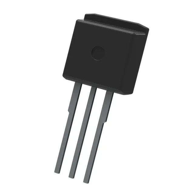
40 V / 100 A N-channel — the conduction-loss floor
The N0434N-S23-AY is a 40 V, 100 A N-channel power MOSFET in a TO-262 through-hole package, built on a standard planar MOSFET process. At 100 A continuous drain current, the package dissipation ceiling of 119 W at the case (Tc) tells you the thermal path to the heatsink is the real limit, not the silicon.
For a 100 kHz switching frequency, the gate-drive power is roughly Qg × Vgs × fsw = 100 nC × 10 V × 100 kHz = 100 mW, well within a standard gate-driver IC's capability.
The TO-262-3 (I²Pak variant with long leads) is a through-hole package intended for a heatsink mount — the 1.5 W dissipation in still air (Ta) versus 119 W at the case (Tc) is the delta between no heatsink and a proper thermal interface. The long leads on the TO-262 allow the part to sit above the PCB for airflow or to reach a chassis-mount heatsink.
It is ROHS3 compliant, with no halogen or lead restrictions beyond the standard exemptions. The ±20 V maximum gate-source voltage is a hard limit; the drive circuit must clamp transients below this rail or the gate oxide ruptures.