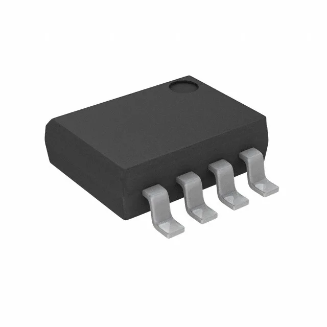
The AT45DB161E-SSHF-B: RoHS3 compliance is confirmed, which simplifies EU and global regulatory acceptance without requiring an exemption review.
Memory architecture and the SPI bus fit
This is a 16 Mbit NOR flash organized as 4096 pages of 528 bytes each — the extra 16 bytes per page (beyond the usual 512) are available for ECC, metadata, or a boot signature without stealing from the main data area. That page layout is specific to the DataFlash family and matters if your firmware expects a standard 512-byte sector erase; the controller must handle the 528-byte page size at the driver level. The SPI interface runs up to 85 MHz, giving a raw read throughput of about 10.6 MB/s in single-I/O mode. For designs that already have an SPI master on the MCU, this part drops in without needing a dedicated parallel-bus controller — the 8-pin SOIC footprint keeps the board routing simple.
Supply voltage and temperature — the operating envelope
If your system runs at 2.5 V core and 3.3 V I/O, this flash can share the 3.3 V rail directly — no level shifter needed on the SPI lines as long as the MCU's I/O voltage is within the same window.
Write timing and the firmware update window
Page write time is 4 ms typical, and a single-byte/word write takes 8 µs. For a 16 Mbit firmware image spread across 4096 pages, the total write time at the page level is about 16 seconds — budget this into the field-update procedure so the system does not brown out or lose power mid-write. The 4 ms page program time is fast enough that a capacitor-backed supply of a few hundred microfarads can ride through a brief glitch.