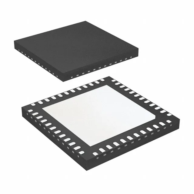
Renesas Electronics 9FGV0841AKILF — Clock & Timing ICs

9FGV0841AKILF PCIe Clock Generator, 100 MHz, 1:9 Fanout

MPN9FGV0841AKILF
End of Life

Renesas 9FGV0841AKILF PCI Express (PCIe) clock generator, PLL Yes, Input Crystal, Output HCSL/LVCMOS, 100 MHz max, 1:9 fanout, 1.7V–1.9V supply, -40°C to 85°C, 48-VFQFN Exposed Pad, Tray.

$4.66Ref. price · indicative, final on quote
Packaging48-VFQFN Exposed Pad
StockContact for availability
MOQ1 pcs
  • 100% new & originalTraceable channels only — no refurbs, no pulls, no remarked parts.
  • Date & lot codes on quoteStated per line before you commit; label photos on request.
  • MSL-compliant ESD packingMoisture-sealed bags with indicator cards; reels photo-verified.
  • PayPal buyer protectionPay by T/T, PayPal or Payoneer — card payments covered end to end.

Specifications

9FGV0841AKILF Technical Specifications
ParameterValue
Mounting typeSurface Mount
Voltage1.7V ~ 1.9V
Frequency100MHz
Operating temperature-40°C ~ 85°C
PLLYes
InputCrystal
OutputHCSL, LVCMOS
PackageTray
Main purposePCI Express (PCIe)
Case48-VFQFN Exposed Pad
Number of circuits1
Ratio - Input:Output1:9
Differential - Input:OutputNo/Yes

Product details

PCIe clock generator with 1:9 fanout

The Renesas 9FGV0841AKILF is a PLL-based clock generator designed specifically for PCI Express (PCIe) reference clock trees. It takes a single crystal input and produces nine differential HCSL or single-ended LVCMOS outputs at up to 100 MHz, covering the reference clock needs of PCIe Gen1, Gen2, and Gen3 root complexes, switches, and endpoints. The 1:9 ratio means one crystal drives nine clock loads — enough for a multi-slot backplane, a switch fabric, or a cluster of PCIe peripherals on a single board. The differential outputs are HCSL, the standard PCIe signalling level, while the LVCMOS option suits legacy or sideband logic. Supply voltage range is 1.7 V to 1.9 V. Operating temperature range is -40°C to 85°C.

100 MHz ceiling and what it means for PCIe generation

Maximum output frequency is 100 MHz, the standard PCIe reference clock rate.

Active lifecycle — no LTB risk

The 9FGV0841AKILF carries an Active lifecycle status with ROHS3 compliance. There is no last-time-buy notice or obsolescence watch on this order code. It can be specified into new designs without a near-term end-of-life concern.

Package and footprint notes

Housed in a 48-VFQFPN with exposed pad, surface-mount only.

Frequently asked questions

What are the alternatives to 9FGV0841AKILF?

The closest functional peer is the 9ZXL0851EKKLF, also a Renesas PCIe clock generator with HCSL outputs and a 1:8 fanout ratio. The 9ZXL0851 runs from a 3.135 V supply (versus 1.7–1.9 V) and supports differential inputs as well as outputs, so a board designed for the 9FGV0841's 1.8 V rail would need a supply change to adopt it. The 9ZXL1231EKILF offers a 1:12 fanout at the same 3.135 V supply. Neither is a drop-in replacement — the supply voltage difference is the deciding factor.