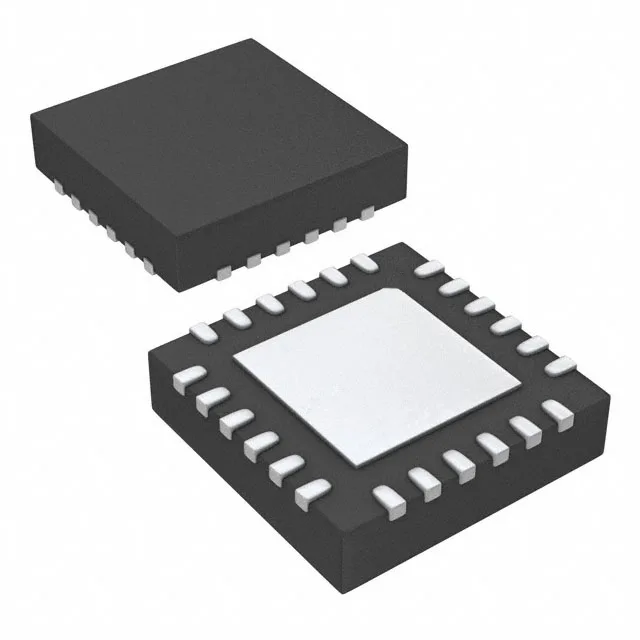
The Renesas 9FGV0231AKILF is a PLL-based clock generator designed specifically for PCI Express (PCIe) reference clock applications. It takes a crystal input and produces up to three output clocks in either HCSL or LVCMOS format, with a maximum output frequency of 100 MHz. The 1:3 input-to-output ratio means one crystal feeds three clock lanes — enough for a small PCIe switch or a root complex with a few downstream ports. The part operates from a 1.7V to 1.9V supply rail and is rated over the -40°C to 85°C industrial temperature range, so it fits in both datacom equipment and outdoor-base-station line cards.
Output standard flexibility — HCSL for PCIe, LVCMOS for general use
The 9FGV0231AKILF supports both HCSL and LVCMOS output types. HCSL (High-Speed Current Steering Logic) is the standard signalling for PCIe reference clocks — if you are feeding a PCIe switch, root complex, or endpoint PHY, you want HCSL. LVCMOS is the fallback for non-PCIe clock distribution on the same board: FPGAs, Ethernet controllers, or generic logic that expects a rail-to-rail CMOS clock. The differential output is enabled only on the HCSL side (the input is single-ended crystal), so the LVCMOS outputs are single-ended. This dual-format capability lets one BOM line cover both the PCIe clock tree and the system-side fanout, reducing oscillator count.
Supply and temperature — industrial-rated, low-voltage rail
The 1.7V to 1.9V supply range is tighter than the typical 3.3V clock generator — this part runs from the 1.8V auxiliary rail common on server and networking motherboards.