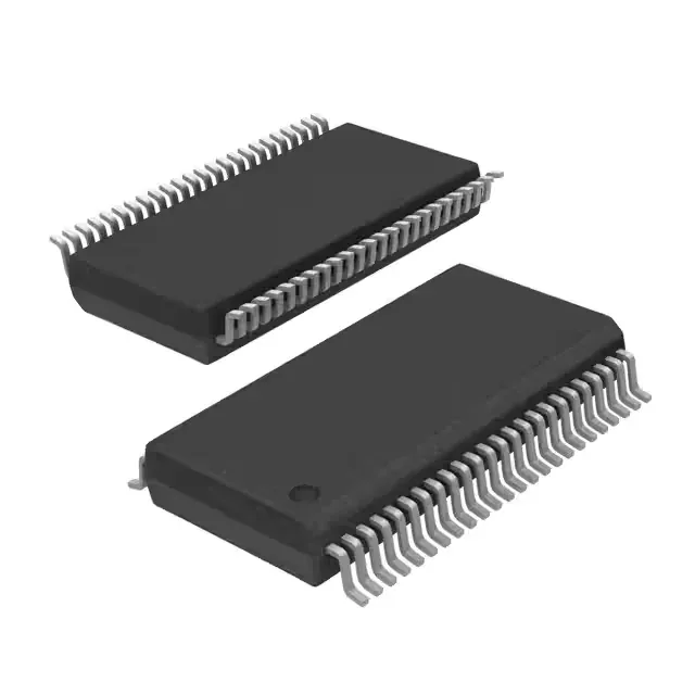
Renesas Electronics 9FG108EGLF — Clock & Timing ICs

9FG108EGLF Renesas Clock Generator IC – 400 MHz, HCSL

MPN9FG108EGLF
End of Life

Renesas 9FG108EGLF, PLL clock generator, 1:9 HCSL outputs, 400 MHz max, 3.135V–3.465V supply, 48-TSSOP, 0°C to 70°C.

$8.7Ref. price · indicative, final on quote
Packaging48-TFSOP (0.240", 6.10mm Width)
StockContact for availability
MOQ1 pcs
  • 100% new & originalTraceable channels only — no refurbs, no pulls, no remarked parts.
  • Date & lot codes on quoteStated per line before you commit; label photos on request.
  • MSL-compliant ESD packingMoisture-sealed bags with indicator cards; reels photo-verified.
  • PayPal buyer protectionPay by T/T, PayPal or Payoneer — card payments covered end to end.

Specifications

9FG108EGLF Technical Specifications
ParameterValue
Mounting typeSurface Mount
Voltage3.135V ~ 3.465V
Frequency400MHz
Operating temperature0°C ~ 70°C
PLLYes
InputClock, Crystal
OutputHCSL
PackageTube
Main purposeIntel CPU Server, PCI Express (PCIe), SATA
Case48-TFSOP (0.240\", 6.10mm Width)
Number of circuits1
Ratio - Input:Output1:9
Differential - Input:OutputNo/Yes

Product details

Server clock tree fanout — one input, nine HCSL lanes

The 9FG108EGLF is a PLL-based clock generator from Renesas designed to produce up to nine HCSL outputs from a single clock or crystal input. It targets Intel CPU server platforms, PCI Express reference clocks, and SATA timing. The 1:9 fanout ratio means one clean reference source can drive multiple PCIe root ports or SATA controllers without adding separate buffers — a common topology on server motherboards where board space is tight and skew between lanes must stay low.

400 MHz ceiling and differential output discipline

Maximum output frequency is 400 MHz, which covers PCIe Gen1 through Gen4 reference clock requirements (100 MHz base with spread-spectrum) and SATA at 150/300/600 MHz rates. The differential output (HCSL) is standard for PCIe — single-ended inputs are accepted, so a crystal or LVCMOS clock source works without level translation. A clean 3.3 V rail with low ripple is expected; sharing this rail with a switching regulator without adequate decoupling can push the PLL jitter above the PCIe mask.

48-TSSOP footprint — reflow and placement notes

Housed in a 48-TFSOP (0.240", 6.10 mm width) package, also listed as 48-TSSOP. The 0.50 mm lead pitch is standard for this density — no exotic stencil or reflow profile required. Check the MSL rating before the first production run; a high MSL level means a bake step before reflow to avoid popcorning. Not rated for extended industrial or automotive temperature ranges.

Frequently asked questions

What is the closest functional second-source for 9FG108EGLF — 9DB803DFLFT?

The 9DB803DFLFT is a peer from Renesas with the same HCSL output type and 400 MHz maximum frequency, but its input-to-output ratio is 1:8 versus the 9FG108EGLF's 1:9. It also accepts differential inputs (Yes/Yes), whereas the 9FG108EGLF accepts only single-ended inputs. Verify your fanout count and input signal type before substituting.

What is the typical application of 9FG108EGLF?

It is designed for Intel CPU server platforms, PCI Express (PCIe) reference clocks, and SATA timing. The 1:9 fanout and HCSL outputs make it suitable for distributing a clean 100 MHz PCIe clock to multiple root ports or controllers on a server motherboard.