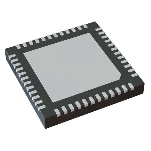
Renesas Electronics 9DBV0841AKLF — Clock & Timing ICs

9DBV0841AKLF PLL Clock Buffer, 1:8 HCSL, 137.5 MHz

MPN9DBV0841AKLF
End of Life

Renesas 9DBV0841AKLF PLL clock buffer, 1:8 HCSL fanout, 137.5 MHz max, 1.7V-1.9V supply, 48-VFQFPN (6x6), 0°C to 70°C.

$4.84Ref. price · indicative, final on quote
Packaging48-VFQFN Exposed Pad
StockContact for availability
MOQ1 pcs
  • 100% new & originalTraceable channels only — no refurbs, no pulls, no remarked parts.
  • Date & lot codes on quoteStated per line before you commit; label photos on request.
  • MSL-compliant ESD packingMoisture-sealed bags with indicator cards; reels photo-verified.
  • PayPal buyer protectionPay by T/T, PayPal or Payoneer — card payments covered end to end.

Specifications

9DBV0841AKLF Technical Specifications
ParameterValue
Mounting typeSurface Mount
Voltage1.7V ~ 1.9V
Frequency137.5MHz
Operating temperature0°C ~ 70°C
PLLYes
InputHCSL
OutputHCSL
PackageTray
Main purposeEthernet, PCI Express (PCIe)
Case48-VFQFN Exposed Pad
Number of circuits1
Ratio - Input:Output1:8
Differential - Input:OutputYes/Yes

Product details

What this PLL clock buffer does on a PCIe or Ethernet line card

The Renesas 9DBV0841AKLF is a PLL-based clock buffer designed to distribute a low-jitter HCSL reference clock from one input to eight outputs. It targets Ethernet switches and PCI Express (PCIe) root complexes where a clean, fanned-out clock keeps link training reliable and bit-error rates low. The part accepts an HCSL input and delivers HCSL outputs, so no level-shifting resistors or translator chips sit between this buffer and the downstream PCIe or Ethernet PHY.

137.5 MHz ceiling and the 1:8 fanout — what they mean for a board

The maximum output frequency is 137.5 MHz. The 1:8 ratio means one input drives eight outputs.

Lifecycle: active — no LTB risk for new production

The 9DBV0841AKLF carries an active lifecycle status. No end-of-life notification, no last-time-buy window to track.

Frequently asked questions

What is the exact function of 9DBV0841AKLF?

The 9DBV0841AKLF is a PLL-based clock buffer that takes one HCSL input and distributes it to eight HCSL outputs, cleaning up jitter and providing a low-skew reference clock for PCI Express and Ethernet applications.

Is 9DBV0841AKLF compatible with PCIe Gen3?

Yes. PCIe Gen3 requires a 100 MHz reference clock with tight jitter specifications. The 9DBV0841AKLF's PLL architecture and HCSL outputs are designed for PCIe clock distribution, and its 137.5 MHz maximum frequency covers the 100 MHz base rate plus spread-spectrum modulation.