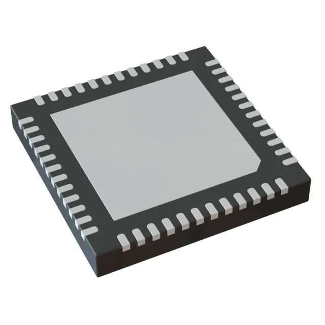
Renesas Electronics 9DBV0831AKLF — Clock & Timing ICs

Renesas 9DBV0831AKLF Clock Buffer, 1:8 HCSL, 137.5 MHz

MPN9DBV0831AKLF
End of Life

Renesas 9DBV0831AKLF, PLL clock buffer, 1:8 HCSL fanout, max 137.5 MHz, for Ethernet and PCI Express, 48-VFQFPN (6x6 mm), 1.7V-1.9V supply, 0°C to 70°C.

$4.84Ref. price · indicative, final on quote
Packaging48-VFQFN Exposed Pad
StockContact for availability
MOQ1 pcs
  • 100% new & originalTraceable channels only — no refurbs, no pulls, no remarked parts.
  • Date & lot codes on quoteStated per line before you commit; label photos on request.
  • MSL-compliant ESD packingMoisture-sealed bags with indicator cards; reels photo-verified.
  • PayPal buyer protectionPay by T/T, PayPal or Payoneer — card payments covered end to end.

Specifications

9DBV0831AKLF Technical Specifications
ParameterValue
Mounting typeSurface Mount
Voltage1.7V ~ 1.9V
Frequency137.5MHz
Operating temperature0°C ~ 70°C
PLLYes
InputHCSL
OutputHCSL
PackageTray
Main purposeEthernet, PCI Express (PCIe)
Case48-VFQFN Exposed Pad
Number of circuits1
Ratio - Input:Output1:8
Differential - Input:OutputYes/Yes

Product details

1:8 HCSL clock buffer with integrated PLL for PCIe and Ethernet reference clocks

The Renesas 9DBV0831AKLF is a 1:8 differential clock buffer with an integrated PLL, accepting one HCSL input and delivering eight HCSL outputs. It is designed to distribute low-jitter reference clocks for PCI Express and Ethernet interfaces in servers, switches, and base stations. The PLL provides jitter attenuation, cleaning up a noisy reference before fanout. Temperature grade is commercial: 0°C to 70°C. This part is intended for indoor, controlled-environment equipment — not suitable for outdoor, industrial, or automotive use without additional qualification.

Active lifecycle — no end-of-life risk for new designs

The 9DBV0831AKLF is listed as Active and ROHS3 compliant.

How it compares to nearby Renesas clock buffers

The 9DB803DFLFT is a 1:8 HCSL fanout buffer with PLL, but it runs at 400 MHz on a 3.135 V supply — a different voltage domain and higher speed tier. The 9DBL411BGLFT has no PLL and only a 1:4 fanout. It is a simpler fanout buffer, not a jitter-cleaning device.

Frequently asked questions

What is the maximum frequency of 9DBV0831AKLF?

The maximum output frequency is 137.5 MHz. This covers PCIe Gen1/2 and common Ethernet reference clock rates (100/125 MHz).

What input signal type does 9DBV0831AKLF require?

The input is HCSL (High-Speed Current Steering Logic), which is the standard differential signaling for PCIe reference clocks. The outputs are also HCSL.

Does 9DBV0831AKLF support PCIe Gen3?

The 137.5 MHz maximum frequency covers PCIe Gen1 and Gen2 base rates. PCIe Gen3 typically uses a 100 MHz reference clock but with tighter jitter requirements. The integrated PLL helps with jitter cleaning, but you must verify that the jitter performance meets your Gen3 link budget. For Gen3/4 designs, consider the 9ZXL0851EKKLF which runs at 400 MHz and has industrial temperature range.