What this 1:8 HCSL clock buffer does on the board
The Renesas 9DBV0831AKILF is a 1:8 differential clock buffer with an integrated PLL, accepting one HCSL input and distributing eight HCSL outputs. It is designed specifically for PCI Express (PCIe) and Ethernet reference clock trees, where low-jitter, frequency-synthesized fanout is required across multiple endpoints. The PLL cleans incoming clock jitter and can multiply or divide the reference frequency, with a maximum output frequency of 137.5 MHz.
Package and footprint — the exposed-pad reality
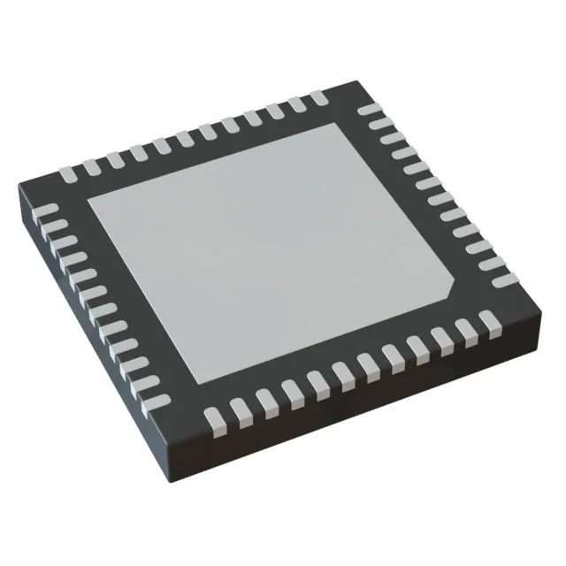
Housed in a 48-VFQFN exposed pad package (6x6 mm body), the 9DBV0831AKILF requires a thermal-via array under the pad for both heat dissipation and a low-inductance ground return. Confirm your assembly house can handle tray-fed QFNs before committing the line.
No last-time-buy window is pending.
How it compares to similar Renesas clock buffers
The 9ZXL0851EKKLF and 9ZXL1231EKILF are higher-frequency siblings (400 MHz max) targeting Intel QPI buses, with a 3.135 V supply rail. The 9DBV0831AKILF operates at 1.7 V–1.9 V and tops out at 137.5 MHz, making it a better fit for PCIe Gen1/2 and 1GbE where lower voltage and moderate speed are the norm. The 9DB803DFLFT is a commercial-temperature (0 °C to 70 °C) variant of the same 1:8 HCSL fanout; the 9DBV0831AKILF extends the temperature range to -40 °C to 85 °C for industrial use.