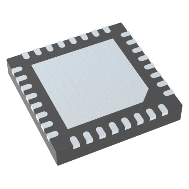
Renesas Electronics 9DBV0441AKLF — Clock & Timing ICs

Renesas 9DBV0441AKLF Clock Buffer, PLL, 1:4 HCSL, 137.5MHz

MPN9DBV0441AKLF
End of Life

Renesas 9DBV0441AKLF, PLL clock buffer, 1:4 HCSL fanout, 137.5 MHz max, 1.7 V to 1.9 V supply, 32-VFQFPN (5x5) exposed pad, 0°C to 70°C.

$3.83Ref. price · indicative, final on quote
Packaging32-VFQFN Exposed Pad
StockContact for availability
MOQ1 pcs
  • 100% new & originalTraceable channels only — no refurbs, no pulls, no remarked parts.
  • Date & lot codes on quoteStated per line before you commit; label photos on request.
  • MSL-compliant ESD packingMoisture-sealed bags with indicator cards; reels photo-verified.
  • PayPal buyer protectionPay by T/T, PayPal or Payoneer — card payments covered end to end.

Specifications

9DBV0441AKLF Technical Specifications
ParameterValue
Mounting typeSurface Mount
Voltage1.7V ~ 1.9V
Frequency137.5MHz
Operating temperature0°C ~ 70°C
PLLYes
InputHCSL
OutputHCSL
PackageTray
Main purposeEthernet, PCI Express (PCIe)
Case32-VFQFN Exposed Pad
Number of circuits1
Ratio - Input:Output1:4
Differential - Input:OutputYes/Yes

Product details

PLL clock buffer for PCIe reference-clock distribution

The Renesas 9DBV0441AKLF is a 1:4 PLL-based clock buffer designed to distribute HCSL reference clocks for Ethernet and PCI Express (PCIe) interfaces. It accepts one HCSL input and delivers four HCSL outputs with integrated PLL cleaning, so the output jitter is lower than the input — useful when a noisy clock source needs cleaning before reaching the PCIe PHY. The part runs from a 1.7 V to 1.9 V supply rail, matching the core voltage of modern server and switch ASICs.

137.5 MHz ceiling — Gen1/Gen2 PCIe, not Gen3

The maximum output frequency is 137.5 MHz, which covers PCIe Gen1 (100 MHz) and Gen2 (100 MHz) reference clocks, plus standard Ethernet frequencies. It does not reach the 400 MHz range needed for PCIe Gen3 or higher-speed serial links — for those, look at the 9ZXL0851EKKLF (400 MHz, 1:8 fanout, industrial temp) or the 9DB803DFLFT (400 MHz, 1:8, 3.135 V supply). The 9DBV0441AKLF is the right fit for 100 MHz PCIe clock trees in server motherboards, switches, and storage controllers that stay within the commercial temperature band.

Active, RoHS3, surface-mount QFN

The part is ROHS3 Compliant, so it meets the latest EU restrictions on hazardous substances. Packaged in a 32-VFQFN with exposed pad (5x5 mm body), it requires a thermal via array under the pad for adequate heat sinking when the buffer is running near its maximum frequency and supply voltage.

Supply and temperature — server-room only

The operating temperature range is 0°C to 70°C, which is commercial grade — suitable for indoor, climate-controlled environments like data-center servers, network switches, and telecom central-office equipment. Not rated for industrial or automotive applications. The supply voltage tolerance (1.7 V to 1.9 V) means the part can share a 1.8 V rail with DDR memory or the core supply of an FPGA or switch ASIC, simplifying the power tree.

Frequently asked questions

Is 9DBV0441AKLF RoHS compliant?

Yes, it is ROHS3 Compliant, meeting the latest EU RoHS directive requirements.

Is 9DBV0441AKLF compatible with PCIe Gen3?

No. The maximum output frequency is 137.5 MHz, which covers PCIe Gen1 and Gen2 reference clocks (100 MHz). PCIe Gen3 requires a 400 MHz-capable buffer such as the 9ZXL0851EKKLF.

What is the replacement for 9DBV0441AKLF?

There is no direct replacement listed. For a higher-frequency alternative with 1:8 fanout and 400 MHz capability, consider the 9ZXL0851EKKLF (industrial temp) or the 9DB803DFLFT (3.135 V supply). Both are PLL-based HCSL buffers but differ in supply voltage, fanout ratio, and temperature range.