1:4 differential fanout buffer for PCIe and QPI clock distribution
The Renesas 9DBL411BGLFT is a 1:4 differential fanout buffer designed to distribute reference clocks for Intel QPI and PCI Express (PCIe) interfaces. It accepts a single HCSL input and delivers four LP-HCSL outputs, maintaining the differential signal integrity required by high-speed serial links. Rated for a maximum frequency of 150 MHz, this buffer sits below the PCIe Gen 1/2/3 reference clock rates — it is sized for the QPI and lower-speed PCIe clock trees where the fanout ratio and output format, not the frequency ceiling, are the selection drivers.
Signal path and fanout architecture
The 1:4 ratio means one input drives four output copies — useful when a single clock source must feed multiple endpoints on the same board without adding separate PLLs per lane. The differential input and output path (Yes/Yes) preserves the common-mode rejection that single-ended distribution loses. Input is HCSL, output is LP-HCSL. LP-HCSL (Low-Power HCSL) reduces the output swing and current draw compared to standard HCSL, which matters when four outputs are active simultaneously on a single 3.0–3.6 V supply rail. The part contains no PLL (PLL: No) — it is a pure fanout buffer. There is no jitter cleaning or frequency synthesis; the output phase noise tracks the input. If the source clock needs cleaning, a PLL-based part like the 9ZXL0851EKKLF or 9ZXL1231EKILF is the correct class.
Package, supply, and temperature grade
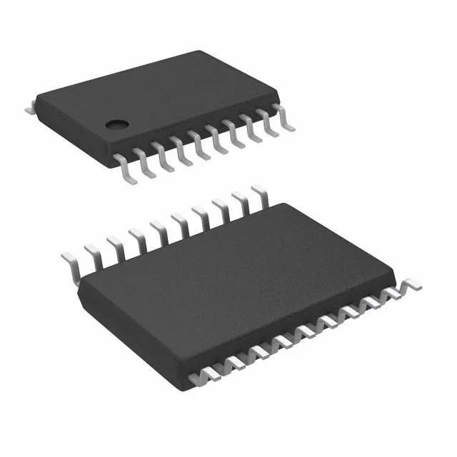
Housed in a 20-TSSOP (4.40 mm width) with a 0.65 mm pitch, the footprint is a standard JEDEC MO-153 variant. The supplier device package is also 20-TSSOP, so no alternate package code to track.
Renesas lists the 9DBL411BGLFT as Active. ROHS3 compliant per the manufacturer's declaration.