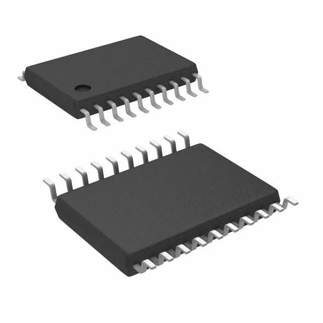
Renesas Electronics 9DBL411BGILFT — Clock & Timing ICs

Renesas 9DBL411BGILFT Clock Fanout Buffer, 150 MHz, LP-HCSL

MPN9DBL411BGILFT
End of Life

Renesas 9DBL411BGILFT, 1:4 differential clock fanout buffer, PLL No, Input HCSL, Output LP-HCSL, 150 MHz max, 3V-3.6V supply, -40°C to 85°C, 20-TSSOP.

$4.31Ref. price · indicative, final on quote
Packaging20-TSSOP (0.173", 4.40mm Width)
StockContact for availability
MOQ1 pcs
  • 100% new & originalTraceable channels only — no refurbs, no pulls, no remarked parts.
  • Date & lot codes on quoteStated per line before you commit; label photos on request.
  • MSL-compliant ESD packingMoisture-sealed bags with indicator cards; reels photo-verified.
  • PayPal buyer protectionPay by T/T, PayPal or Payoneer — card payments covered end to end.

Specifications

9DBL411BGILFT Technical Specifications
ParameterValue
Mounting typeSurface Mount
Voltage3V ~ 3.6V
Frequency150MHz
Operating temperature-40°C ~ 85°C
PLLNo
InputHCSL
OutputLP-HCSL
PackageTape & Reel (TR); Cut Tape (CT)
Main purposeIntel QPI, PCI Express (PCIe)
Case20-TSSOP (0.173\", 4.40mm Width)
Number of circuits1
Ratio - Input:Output1:4
Differential - Input:OutputYes/Yes

Product details

What this clock buffer is and where it fits

The Renesas 9DBL411BGILFT is a 1:4 differential clock fanout buffer designed for Intel QPI and PCI Express (PCIe) reference clock distribution. It takes a single HCSL input and delivers four LP-HCSL outputs, with no PLL in the path — meaning zero added jitter and a fixed, deterministic propagation delay. The part is specified for 150 MHz maximum frequency, covering PCIe Gen 1–3 and QPI clock rates with headroom. It operates from a 3 V to 3.6 V supply and is rated over the industrial temperature range of -40°C to 85°C, making it a fit for outdoor telecom and industrial backplane environments.

Why the PLL-less architecture matters

Because the 9DBL411BGILFT contains no PLL, it does not introduce cycle-to-cycle jitter or phase noise from a VCO. This is a deliberate design choice for applications where the upstream clock source already meets the jitter budget — typically a dedicated oscillator or PLL already on the board. The buffer simply fans out the clean clock to four loads, preserving the signal integrity. The trade-off is that it cannot synthesize a new frequency or clean up a noisy input; it is a pure fanout device.

LP-HCSL output: lower power, same signal swing

The outputs use Low-Power HCSL (LP-HCSL), which maintains the same differential voltage swing as standard HCSL but at reduced current consumption. This is relevant for PCIe clock trees where multiple fanout buffers may be cascaded; the power savings add up. The differential input and output are both rated Yes/Yes, meaning the part can be used in fully differential signal chains without single-ended conversion.

Package and temperature grade for the board

Housed in a 20-TSSOP package (4.40 mm width), the device is surface-mount and occupies minimal board area. The industrial temperature range (-40°C to 85°C) distinguishes it from the commercial-grade 9DBL411BGLFT variant, which is only rated 0°C to 70°C. For designs that must survive cold starts or outdoor enclosures, the 'GILFT' suffix is the correct choice.

Lifecycle and sourcing

The 9DBL411BGILFT is listed as Active in production and ROHS3 compliant.

Frequently asked questions

What is the equivalent to 9DBL411BGILFT?

The closest functional equivalent is the 9DBL411BGLFT, which shares the same pinout, 1:4 fanout, and LP-HCSL outputs, but is rated for commercial temperature (0°C to 70°C) rather than the industrial range of the 'GILFT' variant. For applications requiring a PLL, the 9DB803DFLFT or 9ZXL0851EKKLF are different device classes and not direct substitutes.

Is 9DBL411BGILFT compatible with PCIe?

Yes, the part is designed for PCI Express (PCIe) reference clock distribution, with HCSL input and LP-HCSL output at up to 150 MHz, covering PCIe Gen 1 through Gen 3 requirements.

How to use 9DBL411BGILFT as a clock buffer?

Connect a single HCSL clock source to the input; the device fans it out to four LP-HCSL outputs. Because there is no PLL, no external loop filter or configuration pins are needed — the part is a simple 1:4 fanout with differential I/O.