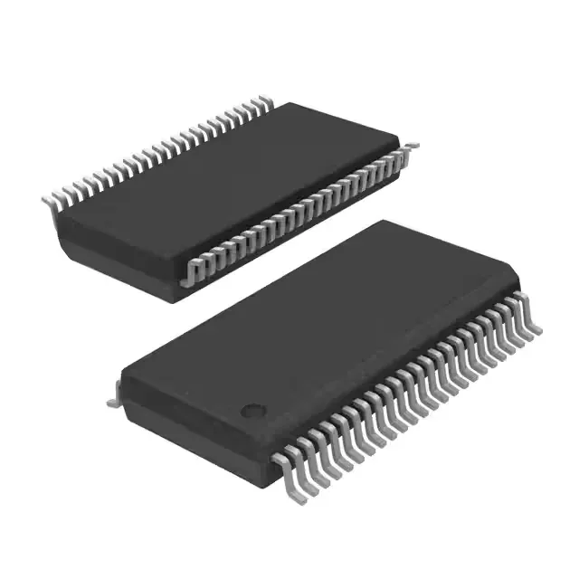
Renesas Electronics 9DB803DGILFT — DC-DC Power Modules

IDT 9DB803DGILFT PCIe Clock Buffer, 1:8 HCSL, 400 MHz

MPN9DB803DGILFT
End of Life

IDT 9DB803DGILFT, PCI Express (PCIe) clock buffer, PLL Yes, Input HCSL, Output HCSL, 1:8 fanout, 400 MHz max, 3.135V–3.465V supply, -40 to 85°C, 48-TSSOP, Tape & Reel.

$5.54Ref. price · indicative, final on quote
Packaging48-TFSOP (0.240", 6.10mm Width)
StockContact for availability
MOQ1 pcs
  • 100% new & originalTraceable channels only — no refurbs, no pulls, no remarked parts.
  • Date & lot codes on quoteStated per line before you commit; label photos on request.
  • MSL-compliant ESD packingMoisture-sealed bags with indicator cards; reels photo-verified.
  • PayPal buyer protectionPay by T/T, PayPal or Payoneer — card payments covered end to end.

Specifications

9DB803DGILFT Technical Specifications
ParameterValue
Mounting typeSurface Mount
Voltage3.135V ~ 3.465V
Frequency400MHz
Operating temperature-40°C ~ 85°C
PLLYes
InputHCSL
OutputHCSL
PackageTape & Reel (TR); Cut Tape (CT)
Main purposePCI Express (PCIe)
Case48-TFSOP (0.240\", 6.10mm Width)
Number of circuits1
Ratio - Input:Output1:8
Differential - Input:OutputYes/Yes

Product details

PCIe clock distribution with PLL cleaning

The Renesas (formerly IDT) 9DB803DGILFT is a 1:8 differential clock buffer with an integrated PLL, purpose-built for PCI Express reference clock trees. It accepts a single HCSL input and delivers eight HCSL outputs at up to 400 MHz, covering PCIe Gen1 through Gen4 and the 400 MHz baseline for Gen5. The PLL cleans incoming jitter and provides deterministic output-to-output skew, which matters when routing clocks to multiple slots or endpoints on a server or switch board. Operating from a 3.135 V to 3.465 V supply and rated from -40°C to 85°C, this buffer suits industrial-temperature networking gear, base stations, and outdoor telecom equipment — not just climate-controlled data centers. The 48-TSSOP package (0.240" body width) keeps the board footprint compact for dense layouts.

What the 400 MHz and 1:8 ratio mean for your BOM

The 400 MHz maximum output frequency covers the PCIe Gen4 reference clock rate (100 MHz multiplied) and the Gen5 baseline. If your design targets Gen5, this buffer meets the frequency requirement. The 1:8 fanout ratio means one input drives eight outputs — enough for a typical motherboard with multiple PCIe slots or a switch card with several downstream ports. The PLL also reduces additive jitter, which is critical for maintaining the tight phase-noise budget of high-speed serial links.

Active lifecycle and sourcing posture

The 9DB803DGILFT carries an Active lifecycle status and is ROHS3 compliant. For a BOM line, this means no near-term obsolescence risk and normal availability through distribution.

Frequently asked questions

Is 9DB803DGILFT compatible with PCIe Gen5?

Yes. The 9DB803DGILFT operates at up to 400 MHz, which meets the PCIe Gen5 reference clock baseline. The PLL-based architecture and HCSL I/O are consistent with the PCIe Gen5 jitter and voltage specifications.

Does 9DB803DGILFT come in a RoHS compliant package?

Yes, the 9DB803DGILFT is ROHS3 compliant per the lifecycle record.

Is 9DB803DGILFT equivalent to 9DB803DGI?

The 9DB803DGILFT is the tape-and-reel ordering variant of the same base device. The suffix 'LF' indicates lead-free / RoHS compliance, and 'T' denotes Tape & Reel packaging. The 9DB803DGI (without the 'T') is the tube/tray variant. Electrically they are identical.