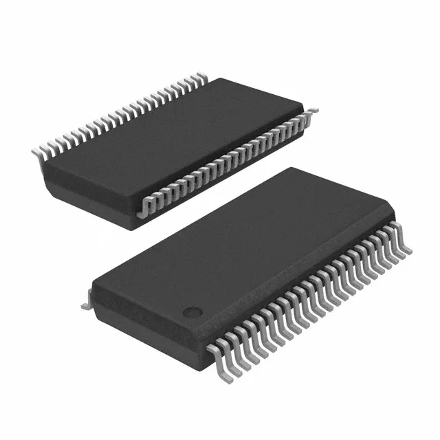
Renesas Electronics 9DB803DFLFT — Microcontrollers & Processors (MCU / MPU / DSP)

Renesas 9DB803DFLFT PCIe Clock Buffer, 400MHz, 1:8, 48-SSOP

MPN9DB803DFLFT
End of Life

Renesas 9DB803DFLFT PCI Express (PCIe) clock buffer, PLL Yes, HCSL input/output, 400MHz max, 1:8 fanout, differential I/O, 48-BSSOP (0.295", 7.50mm Width), surface mount, 3.135V~3.465V supply, 0°C~70°C.

$5.38Ref. price · indicative, final on quote
Packaging48-BSSOP (0.295", 7.50mm Width)
StockIn Stock (27)
Lead timeIn Stock wk
MOQ1 pcs
  • 100% new & originalTraceable channels only — no refurbs, no pulls, no remarked parts.
  • Date & lot codes on quoteStated per line before you commit; label photos on request.
  • MSL-compliant ESD packingMoisture-sealed bags with indicator cards; reels photo-verified.
  • PayPal buyer protectionPay by T/T, PayPal or Payoneer — card payments covered end to end.

Specifications

9DB803DFLFT Technical Specifications
ParameterValue
Mounting typeSurface Mount
Voltage3.135V ~ 3.465V
Frequency400MHz
Operating temperature0°C ~ 70°C
PLLYes
InputHCSL
OutputHCSL
PackageTape & Reel (TR); Cut Tape (CT)
Main purposePCI Express (PCIe)
Case48-BSSOP (0.295\", 7.50mm Width)
Number of circuits1
Ratio - Input:Output1:8
Differential - Input:OutputYes/Yes

Product details

PCIe clock distribution with 1:8 fanout

The Renesas 9DB803DFLFT is a PLL-based clock buffer designed specifically for PCI Express (PCIe) clock distribution, accepting a single HCSL input and delivering eight HCSL outputs with differential signaling throughout. Rated for a maximum frequency of 400 MHz, this buffer supports PCIe Gen1 (2.5 GT/s), Gen2 (5 GT/s), and Gen3 (8 GT/s) reference clock rates — the 400 MHz ceiling covers the 100 MHz nominal PCIe reference clock with margin for spread-spectrum modulation.

Signal integrity and board integration

Differential HCSL signaling on both input and output preserves signal integrity across the clock tree — the 1:8 fanout ratio means a single reference clock source drives up to eight PCIe endpoints without additional buffering stages, reducing jitter accumulation and BOM count. Housed in a 48-BSSOP package (0.295" body width, 7.50 mm) with surface-mount termination, the part fits standard PCIe clock distribution layouts on multi-layer server, storage, and networking boards.

Lifecycle and compliance status

Fully ROHS3 compliant, meeting the latest EU restriction directive for lead-free manufacturing and reflow processes.

Frequently asked questions

What PCIe generations does the 9DB803DFLFT support?

With a 400 MHz maximum frequency, the buffer covers PCIe Gen1, Gen2, and Gen3 reference clock rates (100 MHz nominal with spread-spectrum modulation) — it is not rated for Gen4 or Gen5 which require lower additive jitter and wider bandwidth.

What is the input and output signaling of the 9DB803DFLFT?

Both input and output are HCSL (High-Speed Current Steering Logic) with differential signaling — this is the standard electrical interface for PCIe reference clocks, ensuring compatibility with PCIe root complexes, switches, and endpoint PHYs.

What compliance documentation does Renesas provide for the 9DB803DFLFT?

Renesas provides ROHS3 compliance certification for this part. The standard datasheet includes electrical specifications, jitter performance, and application notes for PCIe clock distribution.