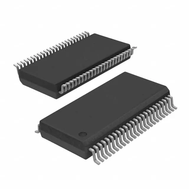
Renesas Electronics 9DB803DFLF — Discrete Semiconductors

Renesas 9DB803DFLF PCIe Clock Buffer, 400 MHz, 1:8 HCSL

MPN9DB803DFLF
End of Life

Renesas 9DB803DFLF PCI Express (PCIe) clock buffer, integrated PLL, 1:8 HCSL fanout, 400 MHz max, 3.135V–3.465V supply, 48-BSSOP (7.50mm width), 0°C to 70°C, Tube.

$5.65Ref. price · indicative, final on quote
Packaging48-BSSOP (0.295", 7.50mm Width)
StockContact for availability
MOQ1 pcs
  • 100% new & originalTraceable channels only — no refurbs, no pulls, no remarked parts.
  • Date & lot codes on quoteStated per line before you commit; label photos on request.
  • MSL-compliant ESD packingMoisture-sealed bags with indicator cards; reels photo-verified.
  • PayPal buyer protectionPay by T/T, PayPal or Payoneer — card payments covered end to end.

Specifications

9DB803DFLF Technical Specifications
ParameterValue
Mounting typeSurface Mount
Voltage3.135V ~ 3.465V
Frequency400MHz
Operating temperature0°C ~ 70°C
PLLYes
InputHCSL
OutputHCSL
PackageTube
Main purposePCI Express (PCIe)
Case48-BSSOP (0.295\", 7.50mm Width)
Number of circuits1
Ratio - Input:Output1:8
Differential - Input:OutputYes/Yes

Product details

PCIe clock distribution with integrated PLL

The Renesas 9DB803DFLF is a one-input, eight-output differential clock buffer for PCI Express (PCIe) reference clock trees. It integrates a PLL, accepts an HCSL input and delivers HCSL outputs. Maximum output frequency is 400 MHz. The 1:8 fanout ratio distributes a clean reference clock to eight PCIe slots, endpoints, or switch ports.

Supply and temperature — indoor equipment only

Supply voltage range is 3.135 V to 3.465 V. Operating temperature is 0°C to 70°C, limiting this part to commercial/indoor environments. Not rated for industrial or automotive under-hood use. If your application needs -40°C to 85°C, the 9ZXL0851EKKLF covers that range with the same 1:8 HCSL fanout and PLL.

Package and mounting — 48-lead SSOP, 7.5 mm wide

Housed in a 48-lead BSSOP (SSOP) package with 0.295 inch (7.50 mm) body width. Surface-mount only. The supplier device package is 48-SSOP. This is a standard footprint for PCIe clock buffers; verify the land pattern against your PCB layout before committing the BOM.

Lifecycle and sourcing — active, no LTB risk

Renesas lists the 9DB803DFLF as Active with ROHS3 compliance. No end-of-life notice, no last-time-buy window. If you are stocking spares for a long-life system, the active status means you can plan replenishment without an EOL scramble.

Frequently asked questions

Is 9DB803DFLF equivalent to 9DB803DFLFT?

The 9DB803DFLFT is the same die and electrical specification as the 9DB803DFLF, but shipped in Tape & Reel (TR) / Cut Tape (CT) / Digi-Reel packaging instead of Tube. Functionally identical; choose the packaging that matches your assembly line.

What is the input and output signal type of 9DB803DFLF?

Both input and output are HCSL (High-Speed Current Steering Logic), the standard differential signaling for PCI Express reference clocks. The part also supports differential input and differential output.

What is the maximum frequency of 9DB803DFLF?

400 MHz.

What are the typical applications of 9DB803DFLF?

PCI Express (PCIe) clock distribution in servers, desktop motherboards, telecom equipment, and test instrumentation. The 1:8 fanout and integrated PLL make it suitable for distributing a jitter-cleaned reference clock to multiple PCIe slots or endpoints.