PCIe clock distribution — 1:4 fanout with integrated PLL
The 9DB433AGLFT is a zero-delay buffer designed to distribute a PCI Express (PCIe) reference clock. It takes one differential clock input and regenerates four HCSL (High-Speed Current Steering Logic) outputs, the standard signaling level for PCIe root complexes, switches, and endpoints. The integrated PLL cleans jitter on the incoming clock and aligns the output edges to the input, maintaining the tight phase-noise budget PCIe Gen1 and Gen2 require. Maximum output frequency is 166 MHz, covering the 100 MHz PCIe reference clock and any integer multiples up to that ceiling.
Supply rail and temperature — indoor equipment only
The narrow tolerance means the board's 3.3 V rail must be regulated — a 3.3 V output from a buck converter with ±2% set-point accuracy stays inside the window; a raw 3.3 V from a linear regulator with ±1% reference is safer. This limits the part to indoor, temperature-controlled environments. No industrial or automotive temperature range is listed; do not spec it into an outdoor base station or engine-bay ECU without active cooling and thermal analysis.
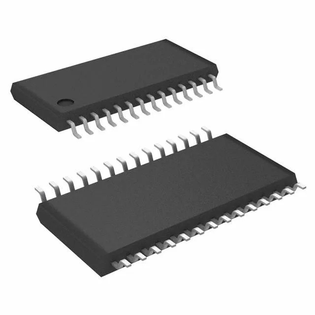
Package and footprint — 28-TSSOP
Housed in a 28-lead TSSOP with 0.65 mm pitch and 4.4 mm body width. The supplier device package is 28-TSSOP. Standard footprint per JEDEC MO-153; no exposed pad, so thermal relief is through the leads only. A 2-layer board routes the differential pairs comfortably if the ground plane is continuous under the package. Cut Tape works for prototypes and small builds.
Lifecycle and compliance — active production
Sourced through independent distribution against an RFQ.