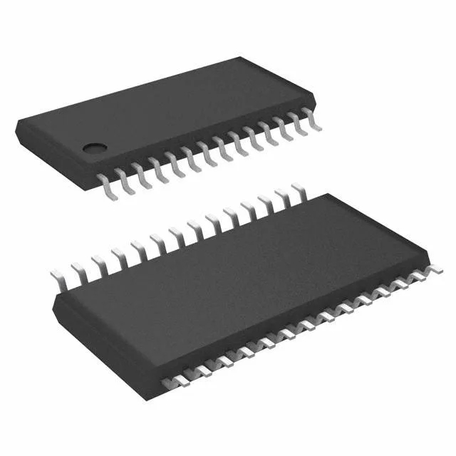
Renesas Electronics 9DB433AGLF — Clock & Timing ICs

9DB433AGLF PCIe Zero-Delay Clock Buffer, 166 MHz, 28-TSSOP

MPN9DB433AGLF
End of Life

Renesas 9DB433AGLF PCI Express (PCIe) zero-delay clock buffer, PLL-based, 1:4 HCSL outputs, 166 MHz max frequency, 3.135V–3.465V supply, 28-TSSOP, 0°C to 70°C.

$4.68Ref. price · indicative, final on quote
Packaging28-TSSOP (0.173", 4.40mm Width)
StockContact for availability
MOQ1 pcs
  • 100% new & originalTraceable channels only — no refurbs, no pulls, no remarked parts.
  • Date & lot codes on quoteStated per line before you commit; label photos on request.
  • MSL-compliant ESD packingMoisture-sealed bags with indicator cards; reels photo-verified.
  • PayPal buyer protectionPay by T/T, PayPal or Payoneer — card payments covered end to end.

Specifications

9DB433AGLF Technical Specifications
ParameterValue
Mounting typeSurface Mount
Voltage3.135V ~ 3.465V
Frequency166MHz
Operating temperature0°C ~ 70°C
PLLYes
InputClock
OutputHCSL
PackageTube
Main purposePCI Express (PCIe)
Case28-TSSOP (0.173\", 4.40mm Width)
Number of circuits1
Ratio - Input:Output1:4
Differential - Input:OutputYes/Yes

Product details

PCIe zero-delay buffer — what it does and where it fits

The Renesas 9DB433AGLF is a PLL-based zero-delay clock buffer designed specifically for PCI Express (PCIe) reference clock distribution. It takes a single differential clock input and regenerates four HCSL (High-Speed Current Steering Logic) outputs with deterministic, low-skew timing — the zero-delay characteristic means the output edges align to the input within the PLL's tracking bandwidth, eliminating the propagation delay you would see from a simple fanout buffer. The 1:4 fanout ratio and 166 MHz maximum frequency cover PCIe Gen1 and Gen2 reference clock requirements. The differential input and output suit it for routing over long traces on a server motherboard or add-in card where common-mode noise rejection matters.

Sourcing and lifecycle — active, no LTB concern

The 9DB433AGLF carries an Active product status and is listed as current lifecycle stage. For BOM-freeze planning, this part is safe for new designs and ongoing production through independent distribution. ROHS3 compliant, so it meets the latest EU restriction requirements without an exemption expiry.

Frequently asked questions

What is the difference between 9DB433AGLF and 9DB433AGLFT?

The suffix 'T' typically denotes Tape & Reel packaging; the 9DB433AGLF ships in Tube. Electrically and functionally they are identical.

Does 9DB433AGLF support PCI Express Gen3?

The 9DB433AGLF is specified for PCI Express (PCIe) as its main purpose and runs at 166 MHz max, which covers the 100 MHz reference clock used by Gen3. However, Gen3 also requires tighter output jitter (typically < 1 ps RMS); verify the datasheet's jitter specification against your Gen3 controller's requirements before committing the BOM.

What is a zero delay buffer?

A zero delay buffer uses a PLL to align its output clock edges to the input reference, effectively cancelling the propagation delay through the device. The 9DB433AGLF does this for PCIe clock distribution, ensuring that downstream devices see the same timing as the source.