PCIe clock distribution with integrated PLL
The Renesas 9DB433AFILF is a zero-delay clock fanout buffer designed specifically for PCI Express (PCIe) reference clock distribution. It integrates a PLL (Phase-Locked Loop) to clean jitter and align the output phases to the input, accepting a single-ended or differential clock input and delivering four HCSL (High-Speed Current Steering Logic) outputs. The maximum output frequency is 166 MHz, and the temperature range is -40°C to 85°C.
This is important for BOM planning: no urgent need to qualify a substitute or stockpile inventory. The part is also ROHS3 compliant, which covers the latest EU RoHS exemption categories.
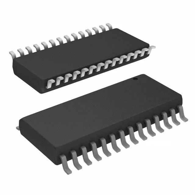
Housed in a 28-SSOP package (0.209" body width, 5.30 mm), the 9DB433AFILF is a surface-mount device. The 28-SSOP footprint is common for clock buffers and fanout devices, so PCB layout reuse from similar parts is straightforward. The part ships in Tube, which is typical for low-volume production or prototyping; for higher-volume reflow, verify the tape-and-reel option if needed.