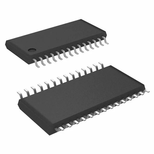
Renesas Electronics 9DB403DGLFT — DC-DC Power Modules

Renesas 9DB403DGLFT PCIe Clock Buffer, 400 MHz, 1:4

MPN9DB403DGLFT
End of Life

Renesas 9DB403DGLFT PCI Express (PCIe) clock buffer, PLL Yes, 1:4 fanout, HCSL input, HCSL/LVDS output, 400 MHz max, 3.135V–3.465V supply, 0°C–70°C, 28-TSSOP.

$4.52Ref. price · indicative, final on quote
Packaging28-TSSOP (0.173", 4.40mm Width)
StockContact for availability
MOQ1 pcs
  • 100% new & originalTraceable channels only — no refurbs, no pulls, no remarked parts.
  • Date & lot codes on quoteStated per line before you commit; label photos on request.
  • MSL-compliant ESD packingMoisture-sealed bags with indicator cards; reels photo-verified.
  • PayPal buyer protectionPay by T/T, PayPal or Payoneer — card payments covered end to end.

Specifications

9DB403DGLFT Technical Specifications
ParameterValue
Mounting typeSurface Mount
Voltage3.135V ~ 3.465V
Frequency400MHz
Operating temperature0°C ~ 70°C
PLLYes
InputHCSL
OutputHCSL, LVDS
PackageTape & Reel (TR); Cut Tape (CT)
Main purposePCI Express (PCIe)
Case28-TSSOP (0.173\", 4.40mm Width)
Number of circuits1
Ratio - Input:Output1:4
Differential - Input:OutputYes/Yes

Product details

What this PCIe clock buffer does on the board

The Renesas 9DB403DGLFT is a 1:4 differential clock buffer with an integrated PLL, designed to clean and fan out a PCI Express reference clock. It takes a single HCSL input and delivers four HCSL or LVDS outputs at up to 400 MHz, covering PCIe Gen1 through Gen3 base frequencies. The 3.135 V to 3.465 V supply rail and 0°C to 70°C operating range target it squarely at commercial server, storage, and networking line cards — not industrial or outdoor gear.

400 MHz ceiling and 1:4 fanout — the fit decision

At 400 MHz max, this buffer handles PCIe Gen3 (8 GT/s) reference-clock duty without margin for Gen4 or Gen5 rates. The 1:4 ratio drives four loads from one input; if your BOM calls for eight downstream devices, the 9DB803DFLFT (1:8, same 400 MHz cap) is the direct drop-in step-up.

Active lifecycle — no last-time-buy watch needed

The 9DB403DGLFT carries an Active product status. That means Renesas continues to manufacture it with no announced end-of-life or last-time-buy window. For a BOM line that needs a stable PCIe clock distribution source, this part does not add obsolescence risk. The ROHS3 compliance is current, and the 28-TSSOP package is a standard footprint that multiple distributors stock.

Sourcing and BOM fit

Because this is an active, commercial-temperature PCIe buffer, it is sourced through standard independent distribution channels. The 28-TSSOP body (4.40 mm width) is a common surface-mount package that reflows on a standard lead-free profile. No special handling or moisture-sensitivity beyond the standard MSL level for TSSOP is expected, but verify the bake requirements if the part has been in storage.

Frequently asked questions

Does 9DB403DGLFT support PCIe Gen4 or Gen5?

No. The 400 MHz maximum frequency covers PCIe Gen1 through Gen3 reference-clock rates. Gen4 (16 GT/s) and Gen5 (32 GT/s) require a buffer with a higher frequency ceiling, such as the 9ZXL0851EKKLF which also operates at 400 MHz but is rated for industrial temperature and Intel QPI alongside PCIe.

What are the cross reference or equivalent parts for 9DB403DGLFT?

For a 1:8 fanout at the same 400 MHz ceiling, the 9DB803DFLFT is the closest functional step-up. For lower-speed applications (150 MHz max), the 9DBL411BGLFT is a 1:4 LP-HCSL buffer without PLL. Both are Renesas parts in similar 28-pin TSSOP packages.

Is 9DB403DGLFT compatible with PCIe Gen3?

Yes. The 400 MHz maximum frequency covers the 100 MHz reference clock used by PCIe Gen3 (8 GT/s). The differential HCSL input and output are standard for that generation.

What is 9DB403DGLFT used for?

It is a 1:4 differential clock buffer with PLL for PCI Express clock distribution on server, storage, and networking line cards. It cleans and fans out a single HCSL reference clock to four HCSL or LVDS loads.