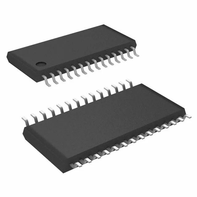
Renesas Electronics 9DB403DGLF — Discrete Semiconductors

Renesas 9DB403DGLF PCIe Clock Buffer, 1:4, 400 MHz, 28-TSSOP

MPN9DB403DGLF
End of Life

Renesas Electronics PCI Express (PCIe) clock buffer, 9DB403DGLF, 1:4 fanout, PLL Yes, HCSL input, HCSL/LVDS outputs, 400 MHz max, 28-TSSOP, ROHS3, Active.

$4.52Ref. price · indicative, final on quote
Packaging28-TSSOP (0.173", 4.40mm Width)
StockContact for availability
Lead timeIn Stock wk
MOQ1 pcs
  • 100% new & originalTraceable channels only — no refurbs, no pulls, no remarked parts.
  • Date & lot codes on quoteStated per line before you commit; label photos on request.
  • MSL-compliant ESD packingMoisture-sealed bags with indicator cards; reels photo-verified.
  • PayPal buyer protectionPay by T/T, PayPal or Payoneer — card payments covered end to end.

Specifications

9DB403DGLF Technical Specifications
ParameterValue
Mounting typeSurface Mount
Voltage3.135V ~ 3.465V
Frequency400MHz
Operating temperature0°C ~ 70°C
PLLYes
InputHCSL
OutputHCSL, LVDS
PackageTube
Main purposePCI Express (PCIe)
Case28-TSSOP (0.173\", 4.40mm Width)
Number of circuits1
Ratio - Input:Output1:4
Differential - Input:OutputYes/Yes

Product details

PCIe clock distribution, 1:4 fanout, 400 MHz ceiling

The 9DB403DGLF is a PLL-based PCI Express (PCIe) clock buffer from Renesas, designed to take a single HCSL reference clock and distribute it to four output copies. The PLL cleans up jitter from the incoming clock, making it suitable for the 100 MHz reference tree in a PCIe root complex to downstream slot endpoints. Outputs are configurable as HCSL or LVDS, giving the layout engineer flexibility to route differential pairs to devices that prefer one standard over the other. The 400 MHz maximum frequency covers PCIe Gen1 through Gen4 base rates (100–400 MHz) with headroom. Supply voltage is 3.135–3.465 V — a tight 3.3 V ±5 % window. The board rail feeding this part must be a regulated supply, not a raw buck output, to stay inside the operating range across load and temperature.

Housed in a 28-TSSOP package with a 4.40 mm body width (0.173"), the 9DB403DGLF mounts on the surface of a standard PCB. The 0.65 mm pin pitch is routable on a 4-layer board without microvias; the differential input and output pairs should be length-matched and impedance-controlled to 100 Ω differential. This part fits enterprise server, storage, and networking gear that lives in a climate-controlled environment.

Frequently asked questions

How does the 9DB403DGLF compare to the 9DB803DFLFT?

Both are PCIe clock buffers in the same Renesas family, with the same supply range, temperature grade, and HCSL/LVDS output capability. The 9DB403DGLF has a 1:4 fanout ratio (one input, four outputs), while the 9DB803DFLFT is a 1:8 fanout (one input, eight outputs). The pinout differs — they are not drop-in replacements without a board spin.