PCIe clock distribution — the 110 MHz PLL buffer for Gen1/2/3 reference trees
The Renesas 9DB233AGLFT is a zero-delay clock fanout buffer built around an integrated PLL, purpose-designed for PCI Express (PCIe) reference clock distribution. It accepts one differential clock input and delivers two HCSL (High-Speed Current Steering Logic) outputs — the standard signaling level for PCIe — at frequencies up to 110 MHz, which covers the 100 MHz reference clock used across PCIe Gen1, Gen2, and Gen3. The 3.3 V nominal supply (3.135 V to 3.465 V) matches the PCIe clock generator rail, and the 1:2 fanout ratio suits small clock trees where two downstream devices (e.g., a root complex and a switch, or two endpoints) need a clean, phase-aligned copy of the reference.
110 MHz ceiling — sized for the PCIe reference, not general-purpose clocking
The 110 MHz maximum frequency is the single most important fit criterion. PCIe reference clocks run at 100 MHz; this part has 10 MHz of headroom above that, which covers the nominal frequency plus spread-spectrum modulation and any tolerance. It will not work as a 125 MHz Ethernet reference or a 156.25 MHz SerDes clock — those need a higher-speed PLL. The 1:2 ratio means exactly two output copies; if your PCIe tree needs three or more fanouts, you either cascade another buffer or step up to a 1:4 or 1:8 part like the 9DB803DFLFT (1:8, 400 MHz capable) or the 9DBL411BGLFT (1:4, LP-HCSL, 150 MHz).
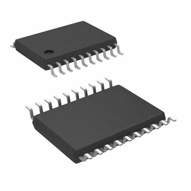
The active lifecycle status means no end-of-life risk for current designs; Renesas continues to manufacture this device in the 20-TSSOP package, and it is ROHS3 compliant with no exemption issues.