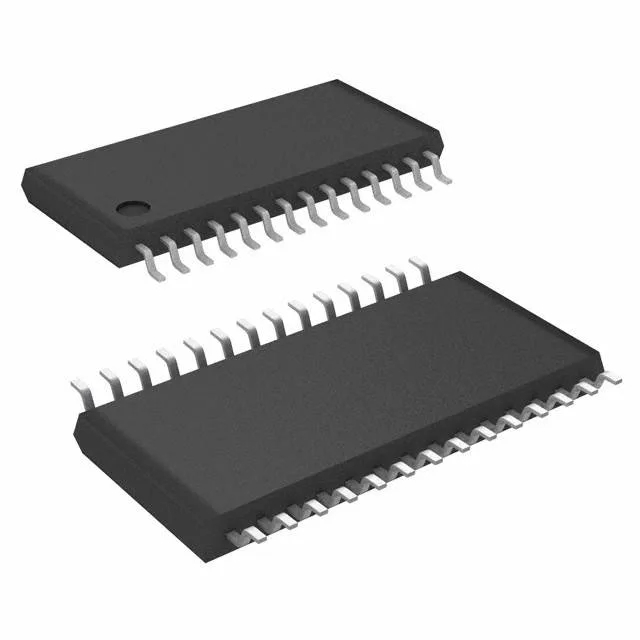
What this PCIe clock buffer does
The Renesas 9DB106BGLFT is a zero-delay PLL buffer designed to distribute a reference clock across a PCI Express (PCIe) clock tree. It takes one differential clock input and delivers six differential HCSL outputs, each capable of driving a separate PCIe slot or endpoint. The integrated PLL cleans up jitter and aligns the output edges to the input, meeting the phase-noise and skew requirements for PCIe Gen1, Gen2, and Gen3 reference clocks.
The 1:6 fanout ratio means one input drives up to six loads — typical for a motherboard with six slots, or a riser card with multiple endpoints. If you need more outputs, the 9DB803DFLFT offers a 1:8 ratio in the same 28-TSSOP footprint.
The ROHS3 compliance is current. If you are freezing a BOM for a multi-year production run, this is a safe choice with no imminent LTB risk.