What this PCIe clock buffer does
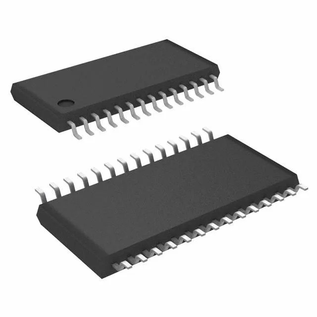
The Renesas 9DB106BGILF is a PLL-based zero-delay clock fanout buffer built for PCI Express reference-clock distribution. It takes one differential clock input and delivers six HCSL outputs, all phase-aligned with low jitter. The PLL cleans up incoming jitter and compensates for board trace delay so every output edge lands in the same window — critical when you're driving multiple PCIe slots or root-complex endpoints off a single oscillator. Rated for 105 MHz maximum, this part covers PCIe Gen1, Gen2, and Gen3 reference-clock requirements. It does not reach the 400 MHz needed for Gen4 or Gen5 — if you're building a Gen4 backplane, look at the 9ZXL0851 or 9ZXL1231 family instead. The 28-TSSOP package is a surface-mount footprint.
Temperature grade and where it runs
If your board lives in a conditioned data-center rack, you could use the commercial-grade 9DB803DFLFT, but this part gives you headroom for the same BOM cost.