PCIe clock distribution — one input, two HCSL outputs
The 9DB102BGLFT is a PLL-based zero-delay buffer from Renesas, purpose-built for PCI Express (PCIe) clock trees. It accepts a single differential clock input and delivers two HCSL (High-Speed Current Steering Logic) outputs — the signalling standard PCIe root complexes and endpoints expect on the reference clock pair. The 1:2 fanout ratio means one input drives exactly two output copies. For a motherboard or add-in card that needs to distribute a 100 MHz PCIe reference clock to two devices (e.g., a CPU and a PCH, or a switch and an FPGA), this buffer covers that split without an external PLL or clock generator.
Supply rail and temperature — commercial-grade constraints
The supply range is 3.135 V to 3.465 V — a tight 3.3 V ±5 % window. This rail should be clean and dedicated; sharing it with a switching regulator or a high-current logic bank risks injecting noise into the PLL's VCO, which shows up as cycle-to-cycle jitter on the HCSL outputs. This part is not qualified for industrial (-40 °C to +85 °C) or automotive environments. If the end system sees an unheated enclosure or engine-bay ambient, this buffer is outside its rated envelope.
Package and board-fit — 20-TSSOP footprint
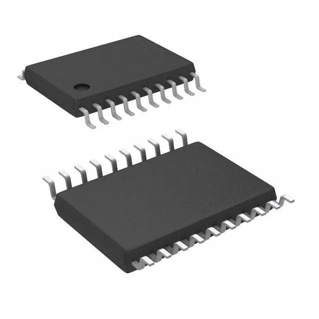
Housed in a 20-TSSOP (4.40 mm width) with 0.65 mm pin pitch. The small footprint keeps the trace length from the buffer to the PCIe slot or endpoint short — important because HCSL edge rates are fast enough that a 1-inch stub on the output can cause reflections that fail the PCIe jitter template. The differential input and outputs are both rated as differential (Yes/Yes per the spec). No single-ended clock conversion is needed on the board — the input pair and each output pair are true differential HCSL.
Lifecycle and compliance — active, RoHS3, no PCN watch
The 20-TSSOP body is MSL-rated per the JEDEC standard; typical MSL for this package family is Level 1 or 2, but the exact floor-life rating should be confirmed from the manufacturer's label on the reel.