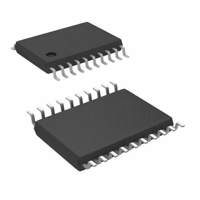
PCIe clock distribution with a 1:2 fanout
The 9DB102BGILF is a zero-delay clock fanout buffer from Renesas, purpose-built for PCI Express (PCIe) reference clock distribution. It takes a single-ended or differential clock input and regenerates two HCSL (High-Speed Current Steering Logic) outputs — the signalling standard required by PCIe root complexes, switches, and endpoints. The internal PLL locks to the input and aligns the output edges to within a few hundred picoseconds of the input, so downstream devices see a clean, low-jitter clock without the cumulative delay of a simple buffer tree. Maximum output frequency is 101 MHz, which covers the 100 MHz PCIe reference clock for Gen1, Gen2, and Gen3 links.
Footprint and board-fit details
The 0.65 mm pin pitch is routable on a standard 4-layer board without microvias; the centre pad is not an exposed thermal pad, so no special copper flooding is required under the package. Because the outputs are HCSL, the AC-coupling capacitors (typically 0.1 µF) must be placed in series with each output trace close to the source — the PCIe Base Spec requires the DC bias to be blocked at the driver side. The input can accept either a differential or single-ended clock; if a single-ended reference is used, the complementary input pin should be biased at the common-mode voltage per the application note.
The device is ROHS3 compliant (lead-free, no exemptions), which covers the current EU RoHS directive and most global environmental regulations. For a BOM that requires a PCIe clock fanout with exactly two outputs, this part is a low-risk, single-source selection. If the design later needs more fanout, the 9ZXL0851EKKLF (1:8, same HCSL output type and industrial temp range) is a pin-compatible upgrade path — but the 9DB102BGILF is the correct fit for a 1:2 requirement and avoids the unused-output termination overhead of a larger fanout part.