Universal frequency translator for high-speed clock trees
The Renesas 8T49N285A-998NLGI is a FemtoClock® NG universal frequency translator that combines a PLL with bypass mode, accepting HCSL, LVCMOS, LVDSM, LVHSTL, LVPECL, or crystal inputs and delivering HSCL, LVCMOS, LVDS, or LVPECL outputs across a 3:8 input-to-output ratio. Its 1 GHz maximum output frequency makes it suited for clock distribution and translation in high-speed networking, telecom line cards, and baseband processing where multiple logic families coexist on the same board.
1 GHz PLL core with bypass — jitter cleaning and test-path flexibility
The integrated PLL (Yes with Bypass) lets the part perform frequency synthesis and jitter attenuation on a reference clock, while the bypass path routes a clean input directly to the output for low-latency test modes or when the PLL is not needed. With a 1 GHz ceiling, this covers most SerDes reference clocks, FPGA transceiver reference clocks, and high-speed ADC/DAC sampling clocks.
Multi-protocol I/O — one part, six input families, four output families
The input stage accepts HCSL, LVCMOS, LVDSM, LVHSTL, LVPECL, and crystal sources — covering the common differential and single-ended standards in wired infrastructure. Outputs are equally flexible: HSCL, LVCMOS, LVDS, LVPECL. That means a single BOM line can bridge between an LVPECL oscillator and an LVDS FPGA bank, or translate a crystal reference to HSCL for a SerDes PHY, without extra level-shifting logic.
Package and footprint — 56-VFQFPN (8x8 mm)
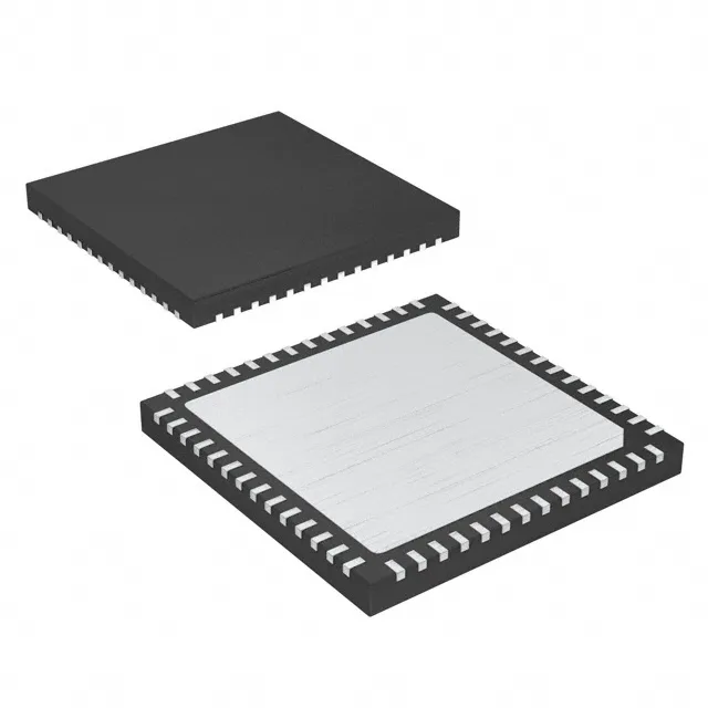
Housed in a 56-lead VFQFN with exposed pad (8x8 mm body).
Renesas lists the 8T49N285A-998NLGI as Active and ROHS3 compliant.