Renesas Electronics 8T49N240-998NLGI — Clock & Timing ICs

8T49N240-998NLGI FemtoClock NG Jitter Attenuator, 867 MHz

MPN8T49N240-998NLGI
End of Life

Renesas FemtoClock® NG series, 8T49N240-998NLGI, PLL-based jitter attenuator, 2:4 fanout, 867 MHz max, LVCMOS/LVDS/LVHSTL/LVPECL/Crystal input, HCSL/LVCMOS/LVDS/LVPECL output, 1.71V–3.465V supply, -40 to 85°C, 40-VFQFPN (6x6).

$19.77Ref. price · indicative, final on quote
Packaging40-VFQFN Exposed Pad
StockContact for availability
MOQ1 pcs
  • 100% new & originalTraceable channels only — no refurbs, no pulls, no remarked parts.
  • Date & lot codes on quoteStated per line before you commit; label photos on request.
  • MSL-compliant ESD packingMoisture-sealed bags with indicator cards; reels photo-verified.
  • PayPal buyer protectionPay by T/T, PayPal or Payoneer — card payments covered end to end.

Specifications

8T49N240-998NLGI Technical Specifications
ParameterValue
TypeJitter Attenuator
SeriesFemtoClock® NG
Mounting typeSurface Mount
Voltage1.71V ~ 3.465V
Frequency867MHz
Operating temperature-40°C ~ 85°C
PLLYes
InputLVCMOS, LVDS, LVHSTL, LVPECL, Crystal
OutputHCSL, LVCMOS, LVDS, LVPECL
PackageTray
Case40-VFQFN Exposed Pad
Divider (Multiplier)Yes/No
Number of circuits1
Ratio - Input:Output2:4
Differential - Input:OutputYes/Yes

Product details

PLL-based jitter attenuator for precision clock trees

The Renesas 8T49N240-998NLGI is a FemtoClock® NG jitter attenuator with an integrated PLL. It accepts LVCMOS, LVDS, LVHSTL, LVPECL, or Crystal inputs and outputs HCSL, LVCMOS, LVDS, or LVPECL. The maximum output frequency is 867 MHz. The input-to-output ratio is 2:4.

Industrial temperature range and supply flexibility

Rated for -40°C to 85°C operation. The supply range spans 1.71 V to 3.465 V.

Package and footprint notes for layout

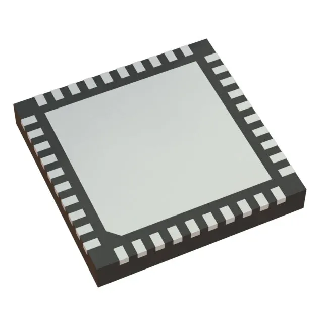
Housed in a 40-VFQFN exposed-pad package (6x6 mm body). The exposed pad must be soldered to a ground plane.

Lifecycle and sourcing posture

The part is ROHS3 compliant. For procurement, this means no immediate supply risk for new designs or production runs.

Frequently asked questions

What are the input and output voltage levels for 8T49N240-998NLGI?

The supply voltage range is 1.71 V to 3.465 V. Input and output logic levels depend on the selected standard — LVCMOS, LVDS, LVHSTL, LVPECL, HCSL — each with its own VOH/VOL or differential swing. The device does not have separate VDDIO rails; the single supply sets the I/O levels for all outputs.