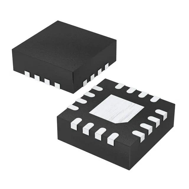
Renesas Electronics 8SLVP2102ANLGI/W — Clock & Timing ICs

Renesas 8SLVP2102ANLGI/W Fanout Buffer, 2 GHz, 16-VFQFN

MPN8SLVP2102ANLGI/W
End of Life

Renesas 8SLVP2102ANLGI/W Fanout Buffer (Distribution), 1:2, 2 GHz max, LVPECL output, CML/LVDS/LVPECL input, 2.375V~3.465V supply, 16-VFQFN Exposed Pad, -40°C~85°C.

$6.63Ref. price · indicative, final on quote
Packaging16-VFQFN Exposed Pad
StockContact for availability
MOQ1 pcs
  • 100% new & originalTraceable channels only — no refurbs, no pulls, no remarked parts.
  • Date & lot codes on quoteStated per line before you commit; label photos on request.
  • MSL-compliant ESD packingMoisture-sealed bags with indicator cards; reels photo-verified.
  • PayPal buyer protectionPay by T/T, PayPal or Payoneer — card payments covered end to end.

Specifications

8SLVP2102ANLGI/W Technical Specifications
ParameterValue
TypeFanout Buffer (Distribution)
Mounting typeSurface Mount
Voltage2.375V ~ 3.465V
Frequency2 GHz
Operating temperature-40°C ~ 85°C
InputCML, LVDS, LVPECL
OutputLVPECL
PackageTape & Reel (TR); Cut Tape (CT)
Case16-VFQFN Exposed Pad
Number of circuits2
Ratio - Input:Output1:2
Differential - Input:OutputYes/Yes

Product details

What this clock buffer does and where it fits

The Renesas 8SLVP2102ANLGI/W is a 1:2 fanout buffer for high-speed clock distribution. It takes a single differential input — CML, LVDS, or LVPECL — and delivers two LVPECL outputs. The part runs up to 2 GHz, so it is aimed at telecom line cards, data-center switches, test equipment, and any board where a clean clock tree needs to split a reference without loading the source. Two independent buffer circuits are inside the 16-VFQFN package, each with its own 1:2 fanout. Supply voltage spans 2.375 V to 3.465 V. The operating temperature range is -40°C to 85°C, so it handles industrial environments — outdoor base stations, motor-drive control boards, and factory-floor Ethernet switches. The 3 mm × 3 mm QFN footprint is compact enough for dense line cards.

2 GHz bandwidth — what it means for your clock tree

A 2 GHz maximum frequency means this buffer can pass high-speed reference clocks without adding jitter from bandwidth limiting. The differential input and output path (Yes/Yes per the spec) means the part preserves common-mode rejection along the clock distribution. That matters when the clock source is across a backplane or through a long cable run where ground noise is a concern.

Signal compatibility — CML, LVDS, LVPECL in, LVPECL out

The input accepts three differential standards: CML, LVDS, and LVPECL. That is useful when the clock source is an FPGA (often LVDS), a high-speed ADC (CML), or a dedicated PLL (LVPECL). The output is always LVPECL, so the downstream receivers must be LVPECL-compatible or you need an AC-coupling network with a DC bias.

Sourcing and lifecycle — active, no LTB worry

ROHS3 compliant. For new designs or BOM fills, there is no last-time-buy pressure. We source it through independent distribution and quote against an RFQ with current availability and pricing confirmed at quote time.

Frequently asked questions

Where can I buy 8SLVP2102ANLGI/W?

This part is sourced to order through independent distribution. Submit an RFQ and we will confirm current availability and pricing at quote time.

Will 8SLVP2102ANLGI/W drop into a panel specified around 8SLVP2108ANLGI/W without rewiring?

No. The 8SLVP2108 has eight LVPECL outputs and a different pinout. The 8SLVP2102 has two outputs in a 16-VFQFN package. A direct swap would require board rework.

What compliance documentation does Renesas provide for 8SLVP2102ANLGI/W?

The part is ROHS3 compliant. Renesas typically provides a RoHS certificate of compliance and a material declaration upon request through the supply chain.