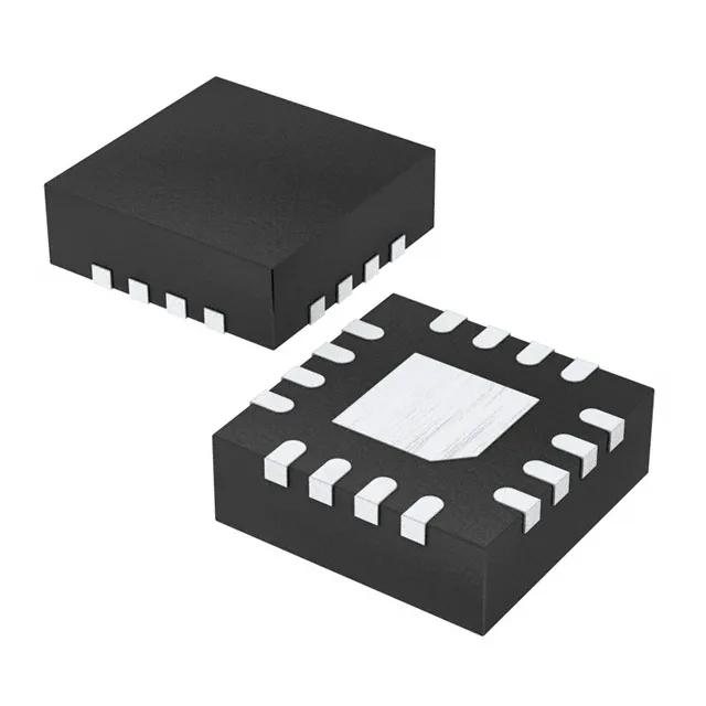
The Renesas 8SLVP1102ANLGI is a 1:2 differential fanout buffer designed to distribute high-speed reference clocks without adding jitter. It accepts CML, LVDS, or LVPECL inputs and produces two LVPECL outputs at up to 2 GHz — the kind of signal a 10+ Gbps SERDES or a high-speed ADC expects.
Supply range and input flexibility
Supply voltage spans 2.375 V to 3.465 V, covering 2.5 V and 3.3 V logic rails. The input stage accepts three differential standards — CML, LVDS, LVPECL — without external level shifting, which simplifies BOM integration when the source is a FPGA bank or a crystal oscillator module. All signal paths are fully differential (input and output), so common-mode noise rejection is inherent; no single-ended mode available.
The 16-VFQFN package (3x3 mm, 0.5 mm pitch) has an exposed thermal pad underneath. On a rework station, the pad needs a stencil aperture big enough to deposit solder paste across the full pad area — a standard QFN profile at 240°C peak works. The part ships in tube, not tape-and-reel, so automated pick-and-place lines need a tube feeder or manual tray loading. No lab, no bench — just a hot-air pencil and a steady hand, but make sure the pad is tinned evenly or the part tilts.
The successor or second-source matrix is straightforward: the 8SLVP1104ANLGI (1:4 fanout, same package and input types) is the closest functional sibling if the design needs four outputs instead of two.