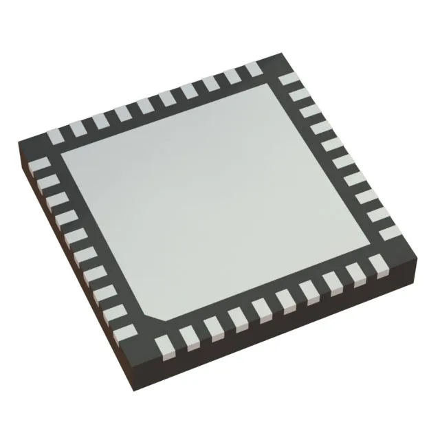
Renesas Electronics 8SLVD1212ANLGI — Clock & Timing ICs

8SLVD1212ANLGI Fanout Buffer, 1:12 LVDS, 2 GHz, 40-VFQFPN

MPN8SLVD1212ANLGI
End of Life

Renesas 8SLVD1212ANLGI Fanout Buffer (Distribution), 1:12 LVDS output, 2 GHz max, accepts CML, LVDS, LVPECL inputs, 2.375V–2.625V supply, -40°C to 85°C, 40-VFQFPN (6x6).

$9.01Ref. price · indicative, final on quote
Packaging40-VFQFN Exposed Pad
RoHSROHS3 Compliant
Independent supplier — new & surplus stockAuthenticity-screened · ESD-safe packingListing updated Aug 2026

Specifications

8SLVD1212ANLGI specifications
ParameterValue
TypeFanout Buffer (Distribution)
MountingSurface Mount
Voltage2.375V ~ 2.625V
Frequency2 GHz
Operating temperature-40°C ~ 85°C
InputCML, LVDS, LVPECL
OutputLVDS
PackageTray
Case40-VFQFN Exposed Pad
Number of circuits1
Ratio - Input:Output1:12
Differential - Input:OutputYes/Yes

Product details

1:12 LVDS fanout buffer for 2 GHz clock trees

The Renesas 8SLVD1212ANLGI is a 1:12 fanout buffer that distributes a single differential clock input to twelve LVDS outputs, rated for frequencies up to 2 GHz. It accepts CML, LVDS, or LVPECL input levels, making it protocol-agnostic at the clock source. The part operates from a 2.375 V to 2.625 V supply and is specified over the industrial temperature range of -40°C to 85°C. Housed in a 40-VFQFPN exposed-pad package (6x6 mm), it suits dense timing boards in telecom infrastructure, data centres, and test equipment where low-jitter clock distribution is required.

The 2 GHz maximum frequency covers high-speed serial interfaces. The 1:12 fanout ratio lets a single oscillator feed twelve downstream receivers.

Active lifecycle, no obsolescence concern

For BOM-freeze planning, this part is qualified for ongoing production and new designs without a near-term end-of-life risk. ROHS3 compliant.

Frequently asked questions

Can 8SLVD1212ANLGI accept CML input?

Yes, the input stage accepts CML, LVDS, and LVPECL levels without external level-shifting.