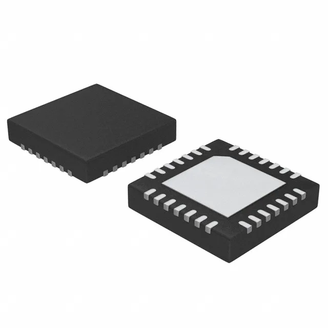
The 8SLVD1208NBGI is a 2:8 fanout buffer and multiplexer from Renesas that takes up to two differential clock inputs (LVDS or LVPECL) and distributes them to eight LVDS outputs at frequencies up to 2 GHz. That 2 GHz ceiling covers most high-speed serial standards — PCIe Gen4/5 reference clocks, 10G Ethernet, and JESD204B SYSREF — without needing a separate redriver. The 2:8 ratio means you can feed two independent clock sources (say, a primary oscillator and a backup PLL) and select between them, or split one input across all eight outputs. The differential input and output path is fully differential end-to-end, so common-mode noise on the clock line gets rejected rather than passed through.
Supply rail and temperature – fitting into an industrial BOM
The part runs on a 2.375 V to 2.625 V supply — a tight 2.5 V nominal rail. That's a narrower tolerance than a generic 3.3 V clock buffer, so the board's 2.5 V rail needs to stay within 5 % regulation. If your system already has a clean 2.5 V plane for SerDes or FPGA transceivers, this buffer drops right in without an extra LDO.
Active production – no end-of-life shadow
For a BOM planner, this removes the single-source clock-buffer risk that often triggers a last-minute respin when a fanout part goes NRND. The package is ROHS3 compliant, no exemption issues for EU or California markets.
Input flexibility – LVDS or LVPECL without level translation
The inputs accept both LVDS and LVPECL levels directly, which saves an external resistor network or AC-coupling cap farm when the source is LVPECL. Many 2 GHz fanout buffers require an external bias network for LVPECL; this one handles it on-chip. The outputs are always LVDS, so the downstream receivers must be LVDS-compatible.