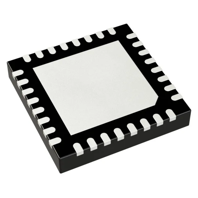
2:8 clock divider for high-speed timing trees
The Renesas 8P79818NLGI is a 2:8 clock divider that accepts CML, HCSL, LVCMOS, LVDS, or LVPECL inputs and delivers the same signal types on eight outputs. It runs up to 700 MHz, making it a fit for distributing reference clocks in networking, base station, and FPGA-based designs where multiple loads need a synchronous, divided clock from one source. The 2:8 ratio means two selectable input paths feed eight outputs — useful for redundant clock sources or for splitting a single clock across multiple line cards without adding external fanout buffers.
The 700 MHz maximum frequency sets the upper bound for the input clock. The differential input and output paths (Yes/Yes) preserve signal integrity at those frequencies, reducing jitter accumulation compared to single-ended distribution.
Signal compatibility — one part, five logic families
The 8P79818NLGI accepts and outputs CML, HCSL, LVCMOS, LVDS, and LVPECL. That means it can sit between a CML oscillator and an LVDS FPGA bank, or between an LVPECL PLL and HCSL fanout — no external level shifters. The 2:8 ratio and wide supply range simplify the BOM for multi-standard clock trees.
Renesas lists the 8P79818NLGI as Active. ROHS3 compliant — no exemptions that would complicate EU or global shipments.