2:12 LVDS fanout at 1.2 GHz — the clock-tree workhorse you don't want to miss
The Renesas 8P34S1212NLGI is a 2:12 fanout buffer and multiplexer that takes CML or LVDS inputs and delivers twelve LVDS outputs at frequencies up to 1.2 GHz. Its 2:12 input-to-output ratio lets you drive a dozen high-speed clock loads from a single device, cutting the component count versus cascading multiple 1:4 or 1:8 buffers — a real board-space win when you're routing a SerDes reference clock or FPGA fabric clock to multiple transceivers.
1.2 GHz — where the timing budget lives or dies
At 1.2 GHz, the period is about 833 ps. Every picosecond of skew or jitter eats into your setup-and-hold margin. The 8P34S1212NLGI's differential LVDS outputs keep the edge rates controlled and the common-mode noise rejection high, which is exactly what you need when fanning a 10-Gigabit Ethernet or PCIe reference clock across a dozen destinations. The 2:12 ratio also means you can route a primary and redundant clock source through the same buffer — the multiplexer function selects between the two inputs, so a single part handles clock redundancy without an external mux.
Package and thermal — the exposed-pad reality
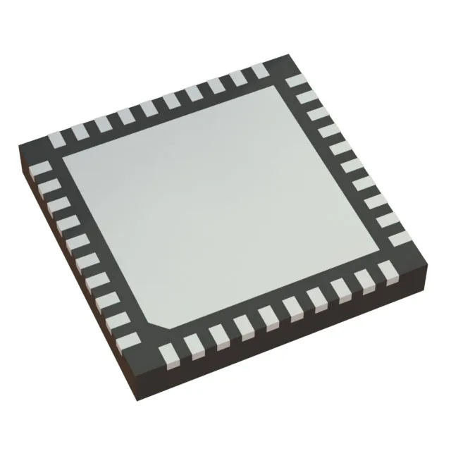
The 40-VFQFN with exposed pad (6x6 mm) is your thermal and ground path. At 1.2 GHz, the part draws a non-trivial current from the 1.8 V rail, and that heat has to go somewhere. Solder the exposed pad to a ground plane with a thermal via array — without it, the junction temperature climbs faster than the datasheet's power-dissipation curves suggest, especially if the ambient hits the 85°C end of the range.