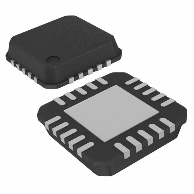
1:6 LVDS fanout buffer for 1.2 GHz clock distribution
The Renesas 8P34S1106NLGI is a 1:6 fanout buffer that accepts CML or LVDS inputs and delivers six LVDS outputs at up to 1.2 GHz. It runs from a single 1.8V nominal supply (1.71V–1.89V) and is housed in a 20-VFQFPN (4x4 mm) package with an exposed pad for thermal relief. Typical use is distributing high-speed reference clocks on SERDES boards, FPGA mezzanines, or datacom line cards where additive jitter and skew matter.
The 1.2 GHz maximum frequency covers reference clock distribution with margin. At these rates the differential LVDS output swing and rise/fall symmetry are specified — the part preserves eye opening across the six fanout paths. The 1:6 ratio lets a single oscillator feed six PLLs or transceiver banks without an external splitter.
The 1.71V–1.89V supply range ties to a clean 1.8V rail — a switching regulator with low ripple is adequate.
It is ROHS3 compliant.