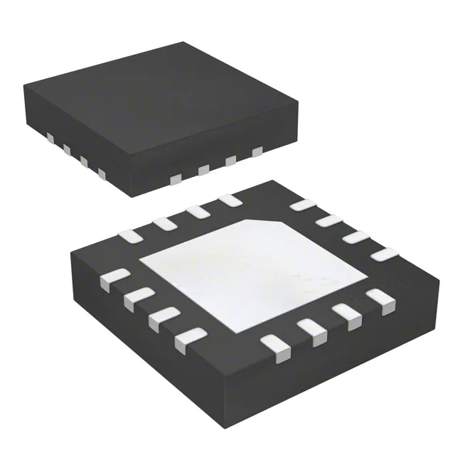
1:2 LVDS fanout buffer for 1.2 GHz clock trees
The Renesas 8P34S1102NLGI is a 1:2 fanout buffer that accepts CML or LVDS inputs and delivers LVDS outputs, rated to 1.2 GHz. It operates from a 1.71V to 1.89V supply rail and is specified across the industrial temperature range of -40°C to 85°C. This buffer is intended for high-speed clock distribution where signal integrity and low additive jitter matter — think SERDES reference clocks, FPGA reference distribution, or data-converter clock trees in telecom and test equipment.
The 1.2 GHz maximum frequency covers high-speed serial standards. The differential LVDS output preserves signal integrity over short board traces. The 1:2 ratio splits one clock into two matched copies.
Supply and signal compatibility
The 1.71V to 1.89V supply range ties this buffer to a 1.8V power rail. Inputs accept both CML and LVDS. The output is LVDS only.
The part is surface-mount only. The exposed pad must be connected to ground plane for both thermal and electrical reasons — floating it can degrade jitter performance at the upper end of the frequency range.
ROHS3 compliant.