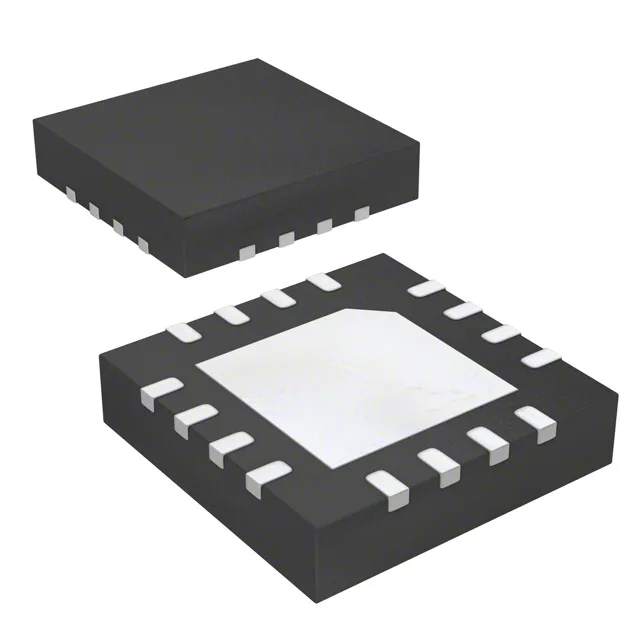
Renesas Electronics 854S01AKILF — Clock & Timing ICs

Renesas 854S01AKILF 2:1 Mux, LVDS/LVPECL Input, 2.5 GHz

MPN854S01AKILF
End of Life

Renesas Electronics 854S01AKILF 2:1 differential multiplexer, LVDS/LVPECL input, LVDS output, 2.5 GHz max, 16-VFQFN exposed pad 3x3 mm, industrial temp -40°C to +85°C, ROHS3.

$12.85Ref. price · indicative, final on quote
Packaging16-VFQFN Exposed Pad
StockContact for availability
Lead timeIn Stock wk
MOQ1 pcs
  • 100% new & originalTraceable channels only — no refurbs, no pulls, no remarked parts.
  • Date & lot codes on quoteStated per line before you commit; label photos on request.
  • MSL-compliant ESD packingMoisture-sealed bags with indicator cards; reels photo-verified.
  • PayPal buyer protectionPay by T/T, PayPal or Payoneer — card payments covered end to end.

Specifications

854S01AKILF Technical Specifications
ParameterValue
TypeMultiplexer
Mounting typeSurface Mount
Voltage3.135V ~ 3.465V
Frequency2.5 GHz
Operating temperature-40°C ~ 85°C
InputLVDS, LVPECL
OutputLVDS
PackageTray
Case16-VFQFN Exposed Pad
Number of circuits1
Ratio - Input:Output2:1
Differential - Input:OutputYes/Yes

Product details

2:1 mux for 2.5 GHz differential clock paths

The 854S01AKILF is a 2:1 differential multiplexer that selects one of two input clock or data signals and routes it to a single LVDS output. It accepts LVDS or LVPECL on the input side and delivers an LVDS-compatible output — the signal standard translation happens inside the mux, so you can feed a LVPECL source into an LVDS receiver without external level shifting. Rated to 2.5 GHz maximum frequency, this part sits in the high-speed serial clock tree where a single reference must be cleanly switched between two sources — for example, selecting between a local oscillator and a recovered clock on a 10 GbE or CPRI line card.

16-VFQFN 3x3 mm — footprint and thermal

Housed in a 16-VFQFN with exposed pad, 3x3 mm body (supplier package 16-VFQFPN). The exposed paddle is the thermal path and the ground return — it must be soldered to a PCB copper pour with via stitching to the inner ground plane. Without that thermal via cluster the junction temperature rises above the 85°C ambient limit when the mux is switching at 2.5 GHz. The 0.50 mm pitch QFN pads fan out to 0.65 mm escape traces on a single inner layer — a two-layer board is feasible if the ground plane under the paddle is continuous. The package height is under 1 mm, so it fits on the back side of a mezzanine card without shadowing the adjacent components. The differential input and output are both rated Yes/Yes, meaning the mux preserves the differential signal path end-to-end; single-ended drive is not supported.

Frequently asked questions

Can 854S01AKILF replace 8SLVP1104ANLGI on the same board?

No — the two parts serve different functions. The 854S01AKILF is a 2:1 multiplexer (selects one of two inputs to one output), while the 8SLVP1104ANLGI is a 1:4 fanout buffer (distributes one input to four outputs). The pinouts, package, and signal flow are different; they are not drop-in substitutes.