1:6 LVDS fanout buffer for high-speed clock trees
The Renesas 854S006AGILF is a 1:6 fanout buffer that accepts a single differential input from HCSL, LVDS, LVHSTL, LVPECL, or SSTL sources and distributes it to six LVDS outputs. It handles clock rates up to 1.7 GHz, making it suitable for distributing reference clocks in high-speed serial links, FPGA reference clocks, and data converter sampling clocks. The device operates from a 2.375V to 3.465V supply and is specified over the -40°C to 85°C industrial temperature range.
Input flexibility and output drive
The input stage accepts five common differential signaling standards — HCSL, LVDS, LVHSTL, LVPECL, and SSTL — so the buffer can sit between a variety of clock generators, oscillators, or SerDes reference outputs without external level translation. The six LVDS outputs provide a low-swing, low-noise fanout that keeps EMI down and signal integrity high over short board traces. Both input and output paths are fully differential, which rejects common-mode noise picked up on the clock distribution path.
The supply voltage range from 2.375V to 3.465V covers both 2.5V and 3.3V rails, so the same BOM line works across systems with different core logic voltages.
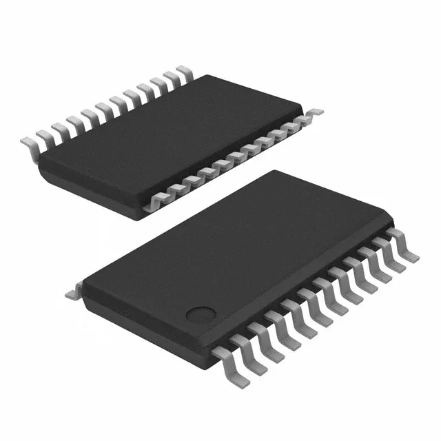
Housed in a 24-lead TSSOP package with a 4.40 mm body width and 0.65 mm pitch, the 854S006AGILF is a surface-mount device that routes easily on standard PCB stacks. The 24-TSSOP footprint is shared across several Renesas fanout buffers, so a layout designed for this part can often accommodate a drop-in alternate if supply conditions change.