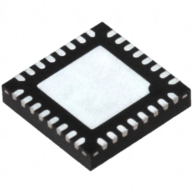
Renesas Electronics 853S111BKILFT — Clock & Timing ICs

Renesas 853S111BKILFT Fanout Buffer, 2:10, 2.5 GHz, 32-VFQFN

MPN853S111BKILFT
End of Life

Renesas 853S111BKILFT, Fanout Buffer (Distribution), Multiplexer, 2:10 ratio, 2.5 GHz max, LVDS/LVPECL/SSTL input, ECL/PECL output, 2.375V–3.8V supply, -40°C to 85°C, 32-VFQFN exposed pad.

$6.8Ref. price · indicative, final on quote
Packaging32-VFQFN Exposed Pad
StockContact for availability
MOQ1 pcs
  • 100% new & originalTraceable channels only — no refurbs, no pulls, no remarked parts.
  • Date & lot codes on quoteStated per line before you commit; label photos on request.
  • MSL-compliant ESD packingMoisture-sealed bags with indicator cards; reels photo-verified.
  • PayPal buyer protectionPay by T/T, PayPal or Payoneer — card payments covered end to end.

Specifications

853S111BKILFT Technical Specifications
ParameterValue
TypeFanout Buffer (Distribution), Multiplexer
Mounting typeSurface Mount
Voltage2.375V ~ 3.8V
Frequency2.5 GHz
Operating temperature-40°C ~ 85°C
InputLVDS, LVPECL, SSTL
OutputECL, PECL
PackageTape & Reel (TR); Cut Tape (CT)
Case32-VFQFN Exposed Pad
Number of circuits1
Ratio - Input:Output2:10
Differential - Input:OutputYes/Yes

Product details

2:10 fanout at 2.5 GHz — what the ratio and frequency mean for your clock tree

The Renesas 853S111BKILFT is a 2:10 differential fanout buffer and multiplexer that accepts LVDS, LVPECL, or SSTL inputs and drives ECL or PECL outputs. Its 2.5 GHz maximum frequency covers 10 GbE reference clocks, JESD204B SYSREF, and RF sampling clocks up to the 2.5 GHz ceiling. The 2:10 fanout ratio means one device can feed ten receiver banks from either of two selectable input sources — useful for redundant clock paths or multi-card backplanes where you need to distribute a clean copy to every slot without adding a second buffer stage.

Supply range and temperature grade — board-level fit

The 2.375 V to 3.8 V supply range lets the 853S111BKILFT run from a 2.5 V or 3.3 V rail directly, which is common in FPGA and SerDes clock domains. The -40°C to 85°C operating temperature covers industrial environments — outdoor telecom cabinets, base stations, and factory-floor equipment where the ambient inside the enclosure can hit 70°C. The 32-VFQFN package with exposed pad (5x5 mm footprint) needs a thermal via pattern under the pad for heat sinking; the datasheet's recommended land pattern is the starting point for the PCB layout.

Input and output standards — what connects where

The input stage accepts three differential families: LVDS (common in FPGA clock outputs), LVPECL (traditional high-speed clock distribution), and SSTL (memory interface clocks). The outputs are ECL or PECL, which are the standard levels for driving clock trees into SerDes transceivers, FPGA clock inputs, and data converters. Because the part is fully differential on both sides, it rejects common-mode noise on long board traces — important when the clock source is on a different card or a distant oscillator.

Lifecycle and sourcing

The 853S111BKILFT is listed as Active and RoHS3 compliant.

Frequently asked questions

What are the input/output standards supported by 853S111BKILFT?

The 853S111BKILFT accepts LVDS, LVPECL, and SSTL differential inputs and drives ECL or PECL outputs. All signal paths are fully differential.

Can I use 853S111BKILFT to replace an IDT part?

The 853S111BKILFT is a Renesas part (Renesas acquired IDT's clock and timing portfolio). It is a direct replacement for the equivalent IDT 853S111I part in the same 2:10 fanout, 2.5 GHz, 32-VFQFN package. Check the pinout against your existing IDT footprint — the datasheet's pin assignment is the final reference.