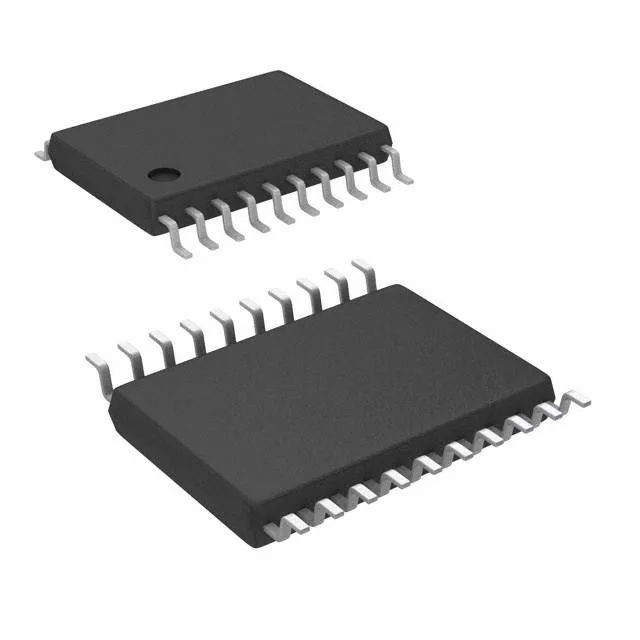
Renesas Electronics 8535AGI-31LF — Clock & Timing ICs

8535AGI-31LF Clock Buffer, 2:4 Fanout, 266 MHz, LVPECL

MPN8535AGI-31LF
End of Life

Renesas 8535AGI-31LF, Fanout Buffer (Distribution), Multiplexer, 2:4 ratio, LVCMOS/LVTTL/Crystal input, LVPECL output, 266 MHz max, 3.135V-3.465V supply, -40°C to 85°C, 20-TSSOP.

$11.73Ref. price · indicative, final on quote
Packaging20-TSSOP (0.173", 4.40mm Width)
StockContact for availability
MOQ1 pcs
  • 100% new & originalTraceable channels only — no refurbs, no pulls, no remarked parts.
  • Date & lot codes on quoteStated per line before you commit; label photos on request.
  • MSL-compliant ESD packingMoisture-sealed bags with indicator cards; reels photo-verified.
  • PayPal buyer protectionPay by T/T, PayPal or Payoneer — card payments covered end to end.

Specifications

8535AGI-31LF Technical Specifications
ParameterValue
TypeFanout Buffer (Distribution), Multiplexer
Mounting typeSurface Mount
Voltage3.135V ~ 3.465V
Frequency266 MHz
Operating temperature-40°C ~ 85°C
InputLVCMOS, LVTTL, Crystal
OutputLVPECL
PackageTube
Case20-TSSOP (0.173\", 4.40mm Width)
Number of circuits1
Ratio - Input:Output2:4
Differential - Input:OutputNo/Yes

Product details

What this clock buffer does that a generic fanout can't

The Renesas 8535AGI-31LF is a 2:4 fanout buffer and multiplexer that takes single-ended inputs — LVCMOS, LVTTL, or a crystal — and delivers LVPECL outputs at up to 266 MHz. That input-to-output conversion is the key differentiator: most clock buffers either pass through differential or single-ended on both sides. Here, the single-ended-to-differential translation happens on-chip, saving an external translator and the associated PCB area and skew. It lives in a 20-TSSOP package, runs from a 3.135V to 3.465V rail, and is rated across the industrial temperature range of -40°C to 85°C.

The 266 MHz ceiling — where it fits and where it doesn't

The 266 MHz maximum frequency sets a clear boundary. This part is sized for PCIe Gen 1 reference clocks, Gigabit Ethernet, FPGA transceiver reference clocks at 125-156.25 MHz, and general-purpose system clock distribution at those rates. It will not retime a 312.5 MHz SerDes reference or a 400 MHz DDR5 clock — those need a higher-speed fanout like the 8SLVP1104 family that runs to 2 GHz. For the 266 MHz and below zone, the 8535AGI-31LF is a clean fit with margin on the edge rates.

Active and available — no LTB clock ticking

The 8535AGI-31LF carries an Active lifecycle status and is ROHS3 compliant. There is no end-of-life notice, no last-time-buy window to track. For a production clock tree that needs to ship for the next several years, this part does not introduce obsolescence risk.

Frequently asked questions

Can the 8535AGI-31LF accept a differential input?

No. The inputs are single-ended only — LVCMOS, LVTTL, or a crystal. The outputs are differential LVPECL. If your clock source is differential (CML, LVDS, LVPECL), consider the 8SLVP1204 which accepts those formats.

What is the closest functional equivalent to the 8535AGI-31LF?

The 8SLVP1204 is a 2:4 fanout buffer and multiplexer with LVPECL outputs, but it accepts differential inputs (CML, LVDS, LVPECL) rather than single-ended. The 8SLVP1104 is a 1:4 fanout with LVPECL outputs and differential inputs. Neither is a drop-in replacement — the input stage differs. For a single-ended-to-LVPECL conversion at 266 MHz, the 8535AGI-31LF is the correct part.