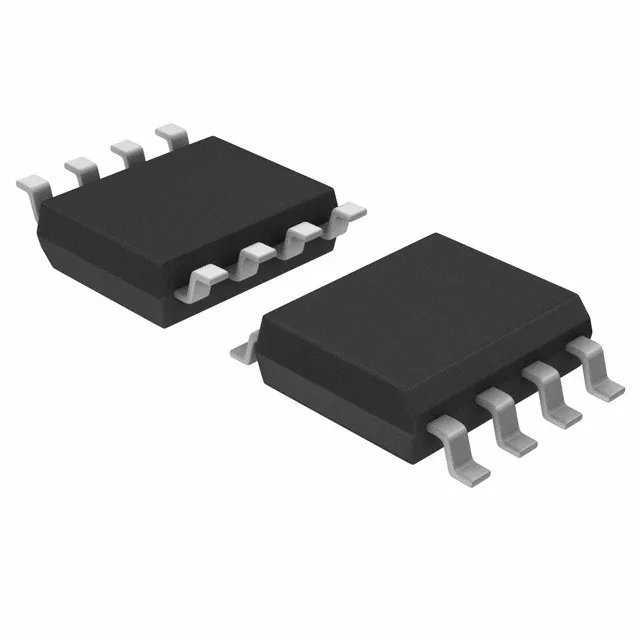
Renesas Electronics 83026BMI-01LF — Clock & Timing ICs

83026BMI-01LF Fanout Buffer 1:2 350MHz 8-SOIC

MPN83026BMI-01LF
End of Life

Renesas 83026BMI-01LF, Fanout Buffer (Distribution), 1:2 ratio, 350 MHz max, HCSL/LVDS/LVHSTL/LVPECL/SSTL input, LVCMOS/LVTTL output, 3.135V-3.465V supply, -40°C to 85°C, 8-SOIC.

$9.5Ref. price · indicative, final on quote
Packaging8-SOIC (0.154", 3.90mm Width)
StockContact for availability
MOQ1 pcs
  • 100% new & originalTraceable channels only — no refurbs, no pulls, no remarked parts.
  • Date & lot codes on quoteStated per line before you commit; label photos on request.
  • MSL-compliant ESD packingMoisture-sealed bags with indicator cards; reels photo-verified.
  • PayPal buyer protectionPay by T/T, PayPal or Payoneer — card payments covered end to end.

Specifications

83026BMI-01LF Technical Specifications
ParameterValue
TypeFanout Buffer (Distribution)
Mounting typeSurface Mount
Voltage3.135V ~ 3.465V
Frequency350 MHz
Operating temperature-40°C ~ 85°C
InputHCSL, LVDS, LVHSTL, LVPECL, SSTL
OutputLVCMOS, LVTTL
PackageTube
Case8-SOIC (0.154\", 3.90mm Width)
Number of circuits1
Ratio - Input:Output1:2
Differential - Input:OutputYes/No

Product details

What this 1:2 clock buffer does on the board

The Renesas 83026BMI-01LF is a single-channel fanout buffer that takes one differential clock input and splits it into two LVCMOS or LVTTL outputs. It handles input standards including HCSL, LVDS, LVHSTL, LVPECL, and SSTL, so it can sit behind most common oscillator or PLL sources without needing a translator. The single 3.3 V supply rail (3.135 V to 3.465 V) keeps the power routing simple on a mixed-signal board. Rated for -40°C to 85°C operation, it fits industrial environments like factory automation controllers, base station timing cards, and test equipment where a clean, low-jitter clock distribution tree matters. The 350 MHz maximum frequency covers most Ethernet, FPGA reference clock, and ADC/DAC sampling clock applications.

350 MHz and the 1:2 fanout — what it means for your timing budget

At 350 MHz, this buffer can distribute a 156.25 MHz or 125 MHz Ethernet reference clock with plenty of margin. The 1:2 ratio means one input drives exactly two loads — useful for splitting a master clock to a pair of FPGAs or to a PHY and a processor without adding a second buffer stage. The differential input accepts a clean LVDS or LVPECL signal from a low-jitter oscillator; the LVCMOS outputs are single-ended, which saves board space but means the output traces need careful impedance control if the run is long. The input:output is differential-to-single-ended, so the input pair is differential but the outputs are standard CMOS levels. This matters when you are driving a clock input that expects LVCMOS levels — no level translation needed on the output side.

8-SOIC package — field-swappable or production solder

Housed in an 8-SOIC (0.154" body width, 3.90 mm wide), this is a hand-solderable, inspection-friendly package. No hot-air station needed for rework — a standard iron with a fine tip and some flux wick will get it off the board clean. Pin pitch is 1.27 mm, so a magnifying lamp is enough to verify solder joints; no microscope required. For a field-service kit, this is the kind of part you can carry a few of and swap on site.

Active production — no end-of-life scramble

The 83026BMI-01LF is listed as Active in production. ROHS3 compliant per, so it meets current European and global environmental requirements.

Frequently asked questions

What input signal types does 83026BMI-01LF accept?

It accepts differential inputs: HCSL, LVDS, LVHSTL, LVPECL, and SSTL. Outputs are single-ended LVCMOS or LVTTL.

Where can I buy 83026BMI-01LF?

This part is sourced to order through independent distribution. Submit an RFQ for current availability and pricing — confirmed at quote time.