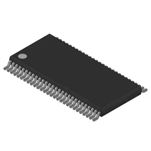
What this 74LVC16344APAG fanout buffer does
The Renesas 74LVC16344APAG is a 74LVC-series fanout buffer (distribution) IC designed to regenerate clock or address signals with minimal skew. It accepts a single clock input per bank and drives four outputs with 3-state capability, giving a 2:4 input-to-output ratio across four internal circuits. The part operates from a 2.3V to 3.6V supply, making it a direct fit for 2.5V and 3.3V logic rails in mixed-voltage systems. Outputs are 3-statable, allowing bus sharing or power-down isolation without external buffers.
The 56-TSSOP package (6.10 mm body width) keeps the board footprint compact for dense backplane or line-card layouts. The differential input/output flag is No/No, so this is a single-ended clock fanout — not intended for LVDS or LVPECL distribution.
What the 2:4 fanout ratio means for your design
With four circuits each providing a 2:4 input-to-output ratio, the 74LVC16344APAG can distribute one clock or address signal to up to four loads per bank, or two signals to two loads each, depending on how the inputs are tied. The 3-state outputs let you disable unused banks to save dynamic power — useful when the same PCB is populated for multiple SKUs with different load counts. The 2.3V to 3.6V supply range covers both 2.5V and 3.3V core logic, but the part is not 5V-tolerant on inputs: feeding a 5V clock into any input exceeds the absolute maximum rating, so level translation is required when interfacing with 5V legacy logic.